|
数据搜索系统,热门电子元器件搜索 |
|
|
数据搜索系统,热门电子元器件搜索 |
|
MB86604LPFV 数据表(PDF) 4 Page - fujitsu semiconductor |
|
|
|||||||||||||||||||||||||||||
MB86604LPFV 数据表(HTML) 4 Page - fujitsu semiconductor |
|
|
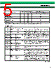
4 / 56 page  4 MB86604L s PIN DESCRIPTION 1. SCSI Interface * : Regarding the status of information transfer which is indicated by MSG, C/D, and I/O pins, See Table Phase Status. Pin number Symbol Pin name I/O Function 60 REQ Request I/O Transfer request signal in the information transfer phases from target to initiator. The input signal to this pin is used for the timing control of data transfer sequence. This is a three-state I/O pin and an active low pin. 68 ACK Acknowledge I/O This pin is for the acknowledge signal from initiator to target for the REQ signal in the information transfer phases. The input signal to this pin is used for the timing control of data transfer sequence. This is a three-state I/O pin and an active low pin. 71 ATN Attention I/O This pin is for the attention signal that initiator requests target for the message transfer phase. This is an active-low pin. 63 MSG* Message I/O This pin is for the message signal that specifies type of information transferred on the data bus. This is an active-low pin and becomes “L” when message phase is specified. 61 C/D* Control/data I/O This pin is for the control/data signal that specifies type of information transferred on the data bus. This an active-low pin and becomes “L” level when command, status, or message phase is specified. 58 I/O* Input/output I/O This pin is for the input/output signal that specifies direction of information transferred on the data bus. This is an active-low pin. When this pin is “L” level, the information is transferred from target to initiator. When this pin is “H” level, the information is transferred from initiator to target. 69 BSY Busy I/O This pin is for the SCSI bus busy signal. In the arbitration phase, this is for the request signal for the use of bus acquisition. This is an active-low pin. 62 SEL Select I/O This pin is for the select signal used by initiator to select target during the selection phase and by target to reselect initiator during the reselection phase. This is an active-low pin. 67 RST Reset I/O This pin is for the reset signal used by any device on the bus. When the device is an input operation, the reset signal is input to this pin. When output operation, the reset signal is output from this pin. This is an active-low pin. 11, 12, 13, 17, 18, 19, 20, 22 DB7 to DB0 Data bus 7 to data bus 0 I/O These pins are for the bidirectional 8-bit SCSI data bus and 1-bit odd parity line. 9DBP Data bus parity |
|
链接网址 |
| ALLDATASHEET是否为您带来帮助? [ DONATE ] |
关于 Alldatasheet | 广告服务 | 联系我们 | 隐私政策 | 数据表链接 | 链接交换 | 制造商名单 All Rights Reserved©Alldatasheet.com |
| Russian : Alldatasheetru.com | Korean : Alldatasheet.co.kr | Spanish : Alldatasheet.es | French : Alldatasheet.fr | Italian : Alldatasheetit.com Portuguese : Alldatasheetpt.com | Polish : Alldatasheet.pl | Vietnamese : Alldatasheet.vn Indian : Alldatasheet.in | Mexican : Alldatasheet.com.mx | British : Alldatasheet.co.uk | New Zealand : Alldatasheet.co.nz |
|
Family Site : ic2ic.com |
icmetro.com |
 Chinese ▼
 English
 Chinese
 German
 Japanese
 Russian
 Korean
 Spanish
 French
 Italian
 Portuguese
 Polish
 Vietnamese
 Indian
 Mexican
 British
 New Zealand