|
数据搜索系统,热门电子元器件搜索 |
|
|
数据搜索系统,热门电子元器件搜索 |
|
AT86RF211DAI-R 数据表(PDF) 23 Page - ATMEL Corporation |
|
|
|||||||||||||||||||||||||||||
AT86RF211DAI-R 数据表(HTML) 23 Page - ATMEL Corporation |
|
|
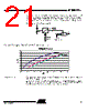
23 / 48 page  23 AT86RF211 1942C–WIRE–06/02 • Register Interface Format A message is made of 3 fields: – address A[3:0]: 4 bits (MSB first) – R/W: read/write selection – data D[31:0]: up to 32 bits (MSB first) Variable register length and partial read or write cycles are supported. In case of partial read or write cycles, the first data (in or out) is always the MSB of the register. • WRITE Mode (R/W = 1) The address, R/W and data bits are clocked on the rising edge of SCK. If the number of data bits is lower than the register capacity, the LSB bits keep their former value allowing safe partial write. If the number of data bits is greater than the reg- ister capacity, the extra bits are ignored. The data is actually written into the register on the rising edge of SLE when the data length is less or equal to the register length. When trying to write more data than the register length, data field is written on the first extra rising clock edge regarding register length. Figure 29. Write Chronogram: Complete Write Cycle in a 10 bits Register The complete register of 10 bits is updated on a rising edge of SLE. Figure 30. Write Chronogram: Partial Write Cycle, Writing 2 bits ADDRESS R/W DATA up to 32 bits (variable length) A[3] A[2] A[1] A[0] R/W MSB D[nbit-1:0] LSB D[8] A[1] A[2] D[7] A[3] R / W SLE SCK SDATA D[6] D[5] D[4] D[3] D[2] D[1] D[0] A[0] D[9] A[1] A[2] A[3] R/W SLE SCK SDATA D[30] A[0] D[31] |
|
链接网址 |
| ALLDATASHEET是否为您带来帮助? [ DONATE ] |
关于 Alldatasheet | 广告服务 | 联系我们 | 隐私政策 | 数据表链接 | 链接交换 | 制造商名单 All Rights Reserved©Alldatasheet.com |
| Russian : Alldatasheetru.com | Korean : Alldatasheet.co.kr | Spanish : Alldatasheet.es | French : Alldatasheet.fr | Italian : Alldatasheetit.com Portuguese : Alldatasheetpt.com | Polish : Alldatasheet.pl | Vietnamese : Alldatasheet.vn Indian : Alldatasheet.in | Mexican : Alldatasheet.com.mx | British : Alldatasheet.co.uk | New Zealand : Alldatasheet.co.nz |
|
Family Site : ic2ic.com |
icmetro.com |
 Chinese ▼
 English
 Chinese
 German
 Japanese
 Russian
 Korean
 Spanish
 French
 Italian
 Portuguese
 Polish
 Vietnamese
 Indian
 Mexican
 British
 New Zealand