|
数据搜索系统,热门电子元器件搜索 |
|
|
数据搜索系统,热门电子元器件搜索 |
|
FT260Q-R 数据表(PDF) 38 Page - Future Technology Devices International Ltd. |
|
|
|||||||||||||||||||||||||||||
FT260Q-R 数据表(HTML) 38 Page - Future Technology Devices International Ltd. |
|
|
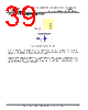
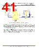
38 / 61 page  Copyright © Future Technology Devices International Limited 38 FT260 HID-CLASS USB TO UART/I2C BRIDGE IC Version 1.1 Document No.: FT_001272 Clearance No.: FTDI#484 7.5 Configuration for System Pins Figure 7.5 Recommended FT260 Configuration of System Pins The pins, DCNF0 and DCNF1, will determine one of 3 configurations for the FT260 as defined in Section 5.1. These 2 pins have internal pull-down resistors; these 2 pins can be left floating for logic-0. If logic-1 is applied for DCNF0 and/or DCNF1, a 10K Ohm resistor should be connected to VCCIO as shown in Figure7.5. The pin RESETN is the external reset source for the FT260. There is also a power-on-reset (POR) design in the FT260. If there is no requirement for an external reset, RESETN can be left floating or weakly tied to logic-high. If an external reset is required in the design, the related circuit in Figure 7.5 can be used for reference. The DEBUGGER pin is reserved for debugging purposes and should be tied to VCCIO, the I/O power domain for the FT260. The pin, STEST_RESETN, is also a reserved pin and should be tied to logic-high. Note that the GND pin located at pin-29 in Figure 7.5 is the paddle in the bottom side of the WQFN28 package. It should be tied together with the GND for FT260. |
|
链接网址 |
| ALLDATASHEET是否为您带来帮助? [ DONATE ] |
关于 Alldatasheet | 广告服务 | 联系我们 | 隐私政策 | 数据表链接 | 链接交换 | 制造商名单 All Rights Reserved©Alldatasheet.com |
| Russian : Alldatasheetru.com | Korean : Alldatasheet.co.kr | Spanish : Alldatasheet.es | French : Alldatasheet.fr | Italian : Alldatasheetit.com Portuguese : Alldatasheetpt.com | Polish : Alldatasheet.pl | Vietnamese : Alldatasheet.vn Indian : Alldatasheet.in | Mexican : Alldatasheet.com.mx | British : Alldatasheet.co.uk | New Zealand : Alldatasheet.co.nz |
|
Family Site : ic2ic.com |
icmetro.com |
 Chinese ▼
 English
 Chinese
 German
 Japanese
 Russian
 Korean
 Spanish
 French
 Italian
 Portuguese
 Polish
 Vietnamese
 Indian
 Mexican
 British
 New Zealand