|
数据搜索系统,热门电子元器件搜索 |
|
|
数据搜索系统,热门电子元器件搜索 |
|
HCV1707R1-R48-R 数据表(PDF) 23 Page - Vicor Corporation |
|
|
|||||||||||||||||||||||||||||
HCV1707R1-R48-R 数据表(HTML) 23 Page - Vicor Corporation |
|
|
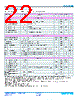
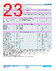
23 / 41 page  Cool-Power® ZVS Switching Regulators Rev 1.5 Page 23 of 41 03/2018 PI352x-00 PI3526-00 (12VOUT) Electrical Characteristics (Cont.) Specifications apply for –40°C < TINT < 120°C, VIN = 48V, EN = High, unless otherwise noted. Parameter Symbol Conditions Min Typ Max Unit Timing Switching Frequency fs [f] While in DCM operating mode only, SYNCI grounded 658 700 742 kHz Fault Restart Delay tFR_DLY 30 ms Synchronization Input (SYNCI) Synchronization Frequency Range fSYNCI –50% and +10% relative to set switching frequency (fS), while in DCM operating mode only. [c] [f] 350 770 kHz SYNCI Threshold VSYNCI 2.5 V Synchronization Output (SYNCO) SYNCO High VSYNCO_HI Source 1mA 4.5 V SYNCO Low VSYNCO_LO Sink 1mA 0.5 V SYNCO Rise Time tSYNCO_RT 20pF load 10 ns SYNCO Fall Time tSYNCO_FT 20pF load 10 ns Soft Start, Tracking and Error Amplifier TRK Active Range (Nominal) VTRK 0 1.4 V TRK Enable Threshold VTRK_OV 20 40 60 mV TRK to EAIN Offset VEAIN_OV 50 80 110 mV Charge Current (Soft Start) ITRK 30 50 70 µA Discharge Current (Fault) ITRK_DIS VTRK = 0.5V 8.7 mA TRK Capacitance, Internal CTRK_INT 47 nF Soft-Start Time tSS CTRK_EXT = 0µF 0.6 0.94 1.6 ms Error Amplifier Trans-Conductance GMEAO [b] 7.6 mS PSM Skip Threshold PSMSKIP [b] 0.8 V EAIN Capacitance, Internal CEAIN-INT 56 pF Error Amplifier Output Impedance ROUT [b] 1 MΩ Internal Compensation Capacitor CHF [b] 56 pf Internal Compensation Resistor RZI [b] 5 kΩ [a] All parameters reflect regulator and inductor system performance. Measurements were made using a standard PI352x evaluation board with 3 x 3" dimensions and 4 layer, 2oz copper. Refer to inductor pairing table within Application Description section for specific inductor manufacturer and value. [b] Regulator is assured to meet performance specifications by design, test correlation, characterization, and/or statistical process control. Output voltage is determined by an external feedback divider ratio. [c] Output current capability may be limited and other performance may vary from noted electrical characteristics when VOUT is not set to nominal. [d] Refer to Output Ripple plots. [e] Refer to Load Current vs. Ambient Temperature curves. [f] Refer to Switching Frequency vs. Load current curves. [g] Contact factory applications for array derating and layout best practices to minimize sharing errors. |
|
链接网址 |
| ALLDATASHEET是否为您带来帮助? [ DONATE ] |
关于 Alldatasheet | 广告服务 | 联系我们 | 隐私政策 | 数据表链接 | 链接交换 | 制造商名单 All Rights Reserved©Alldatasheet.com |
| Russian : Alldatasheetru.com | Korean : Alldatasheet.co.kr | Spanish : Alldatasheet.es | French : Alldatasheet.fr | Italian : Alldatasheetit.com Portuguese : Alldatasheetpt.com | Polish : Alldatasheet.pl | Vietnamese : Alldatasheet.vn Indian : Alldatasheet.in | Mexican : Alldatasheet.com.mx | British : Alldatasheet.co.uk | New Zealand : Alldatasheet.co.nz |
|
Family Site : ic2ic.com |
icmetro.com |
 Chinese ▼
 English
 Chinese
 German
 Japanese
 Russian
 Korean
 Spanish
 French
 Italian
 Portuguese
 Polish
 Vietnamese
 Indian
 Mexican
 British
 New Zealand