|
数据搜索系统,热门电子元器件搜索 |
|
|
数据搜索系统,热门电子元器件搜索 |
|
HCV1707R1-R48-R 数据表(PDF) 37 Page - Vicor Corporation |
|
|
|||||||||||||||||||||||||||||
HCV1707R1-R48-R 数据表(HTML) 37 Page - Vicor Corporation |
|
|
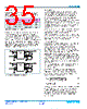
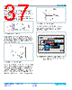
37 / 41 page  Cool-Power® ZVS Switching Regulators Rev 1.5 Page 37 of 41 03/2018 PI352x-00 Layout Guidelines To optimize maximum efficiency and low noise performance from a PI352x-00 design, layout considerations are necessary. Reducing trace resistance and minimizing high current loop returns along with proper component placement will contribute to optimized performance. A typical buck converter circuit is shown in Figure 97. The potential areas of high parasitic inductance and resistance are the circuit return paths, shown as LR below. The path between the COUT and CIN capacitors is of particular importance since the AC currents are flowing through both of them when Q1 is turned on. Figure 98, schematically, shows the reduced trace length between input and output capacitors. The shorter path lessens the effects that copper trace parasitics can have on the PI352x-00 performance. When Q1 is on and Q2 is off, the majority of CIN’s current is used to satisfy the output load and to recharge the COUT capacitors. When Q1 is off and Q2 is on, the load current is supplied by the inductor and the COUT capacitor as shown in Figure 99. During this period CIN is also being recharged by the VIN. Minimizing CIN loop inductance is important to reduce peak voltage excursions when Q1 turns off. Also, the difference in area between the CIN loop and COUT loop is vital to minimize switching and GND noise. Figure 100 illustrates the tight path between CIN and COUT (and VIN and VOUT) for the high AC return current. The PI352x-00 evaluation board uses a layout optimized for performance in this way. C OUT C IN V IN Figure 97 — Typical Buck Regulator C OUT V IN C IN Figure 98 — Current flow: Q1 closed C OUT V IN C IN Figure 99 — Current flow: Q2 closed PGND PGND VOUT VS1 VIN Inductor ZVS- Buck SIP Figure 100 — Recommended layout for Optimized AC Current within the SiP, Inductor, and Ceramic Input and Output Capacitors |
|
链接网址 |
| ALLDATASHEET是否为您带来帮助? [ DONATE ] |
关于 Alldatasheet | 广告服务 | 联系我们 | 隐私政策 | 数据表链接 | 链接交换 | 制造商名单 All Rights Reserved©Alldatasheet.com |
| Russian : Alldatasheetru.com | Korean : Alldatasheet.co.kr | Spanish : Alldatasheet.es | French : Alldatasheet.fr | Italian : Alldatasheetit.com Portuguese : Alldatasheetpt.com | Polish : Alldatasheet.pl | Vietnamese : Alldatasheet.vn Indian : Alldatasheet.in | Mexican : Alldatasheet.com.mx | British : Alldatasheet.co.uk | New Zealand : Alldatasheet.co.nz |
|
Family Site : ic2ic.com |
icmetro.com |
 Chinese ▼
 English
 Chinese
 German
 Japanese
 Russian
 Korean
 Spanish
 French
 Italian
 Portuguese
 Polish
 Vietnamese
 Indian
 Mexican
 British
 New Zealand