|
数据搜索系统,热门电子元器件搜索 |
|
|
数据搜索系统,热门电子元器件搜索 |
|
P9221-R3 数据表(PDF) 23 Page - Renesas Technology Corp |
|
|
|||||||||||||||||||||||||||||
P9221-R3 数据表(HTML) 23 Page - Renesas Technology Corp |
|
|
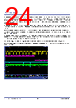
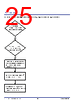
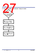
23 / 46 page  P9221-R3 Datasheet © 2017 Integrated Device Technology, Inc. 23 October 20, 2017 10. Bi-directional User Data Communication In customer end systems, the transmitter and receiver boards need to have an external microcontroller (MCU) or leverage an existing application processor to orchestrate bi-directional communication. Using the I2C communication, the MCU on the receiver board needs to load the data into specific registers and trigger the communication. The P9221-R3 sends the data to the P9242-R3 using amplitude-shift keying (ASK) modulation. The P9242-R3 will receive the data and interrupt the MCU on the transmitter when the data is ready to be read. The external MCU on the transmitter follows the same procedure to send the data to the P9221-R3. When new data is available to be read, the P9221-R3 will interrupt the external MCU on the receiver board. Bi-directional user data communication is enabled only in the power transfer phase for the WPC standard. The external MCU on the receiver board can read register 014AHEX to determine whether the P9221-R3 is in the power transfer phase. Register 014AHEX will be set to 5HEX when the device is in the power transfer phase. See Figure 25 for a state diagram that illustrates the procedure that the external MCU on the receiver board must follow to send the user data from the P9221-R3 to the P9242-R3 as described in section 10.1. See Figure 26 for a state diagram that illustrates the procedure the external MCU must follow to read the data sent by the P9242-R3 as described in section 10.2. 10.1 Transferring Data from the P9221-R3 to the P9242-R3 The external MCU on the receiver board should read bit 0 in register 004EHEX to determine the status of the communication channel before initiating a new transfer. If the communication channel is free, bit 0 in register 004EHEX is 0. If the communication channel is busy, bit 0 in register 004EHEX is set to 1. The P9221-R3 receiver supports sending up to 8 bytes of user data. The external MCU on the receiver should write the data that it will be sending to the transmitter into outgoing data registers (0089HEX to 0090HEX) and set the Data Header register (0088HEX) accordingly. The Data Header register (see Table 29) indicates the number of bytes that need to be transmitted. For example, if the external MCU on the receiver intends to transfer 3 bytes of information, it should write 38HEX to register 0088HEX and write the user data into registers 0089HEX to 008BHEX. The P9221-R3 will not transfer registers 008CHEX to 0090HEX when the header is set to 3 bytes. If the external MCU on the receiver will be sending 8 bytes of information, it should write 88HEX to register 0088HEX and write the data into registers 0089HEX to 0090HEX. Table 9. Registers Used for Data Transmission from P9221-R3 to P9242-R3 Register Register Address Command Register 004EHEX Data Header Register 0088HEX Outgoing User Data Registers 0089HEX to 0090HEX (8 bytes) WPC Power Transfer Phase Indicator 014AHEX The external MCU on the receiver should set bit 0 in the Command register 004EHEX to 1 for triggering the communication after loading the user data into the outgoing data registers and setting the data header for the correct number of bytes. After receiving the communication trigger from the control register, the P9221-R3 reads the data header register and outgoing data registers and constructs a proprietary communication packet with a packet checksum. The communication packet is sent into the channel between two Control Error Packets (CEP) using ASK modulation. Figure 23 shows the timing diagram for the user data transfer from the P9221-R3 to the P9242-R3. Figure 23. Timing Diagram for a User Data Transfer from the P9221-R3 to the P9242-R3 CEP Packet CEP Packet Proprietary Communication Packets (ASK) |
|
链接网址 |
| ALLDATASHEET是否为您带来帮助? [ DONATE ] |
关于 Alldatasheet | 广告服务 | 联系我们 | 隐私政策 | 数据表链接 | 链接交换 | 制造商名单 All Rights Reserved©Alldatasheet.com |
| Russian : Alldatasheetru.com | Korean : Alldatasheet.co.kr | Spanish : Alldatasheet.es | French : Alldatasheet.fr | Italian : Alldatasheetit.com Portuguese : Alldatasheetpt.com | Polish : Alldatasheet.pl | Vietnamese : Alldatasheet.vn Indian : Alldatasheet.in | Mexican : Alldatasheet.com.mx | British : Alldatasheet.co.uk | New Zealand : Alldatasheet.co.nz |
|
Family Site : ic2ic.com |
icmetro.com |
 Chinese ▼
 English
 Chinese
 German
 Japanese
 Russian
 Korean
 Spanish
 French
 Italian
 Portuguese
 Polish
 Vietnamese
 Indian
 Mexican
 British
 New Zealand