|
数据搜索系统,热门电子元器件搜索 |
|
|
数据搜索系统,热门电子元器件搜索 |
|
P9242-R3 数据表(PDF) 22 Page - Renesas Technology Corp |
|
|
|||||||||||||||||||||||||||||
P9242-R3 数据表(HTML) 22 Page - Renesas Technology Corp |
|
|
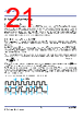
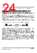
22 / 44 page  P9242-R3/RB Datasheet © 2019 Integrated Device Technology, Inc. 22 May 17, 2019 Each byte will comply with the start, data, parity, and stop asynchronous serial format structure shown in Figure 20: Figure 20. Example of Asynchronous Serial Byte Format for FSK Start Stop Parity b0 1 2 3 4 5 6 7 b b b b b b b 8.3 Bit Decoding Scheme for ASK As required by the WPC, the P9242-R3 uses a differential bi-phase coding scheme to demodulate data bits from the power signal. A clock frequency of 2kHz is used for this purpose. A logic ONE bit is encoded using two narrow transitions, whereas a logic ZERO bit is encoded using one wider transition as shown in Figure 21. Figure 21. Bit Decoding Scheme t CLK ONE ZERO ONE ZERO ONE ONE ZERO ZERO 8.4 Byte Decoding for ASK Each byte in the communication packet comprises 11 bits in an asynchronous serial format, as shown in Figure 22. Each byte has a start bit, 8 data bits, a parity bit, and a single stop bit. Figure 22. Byte Decoding Scheme Start Stop Parity b0 1 2 3 4 5 6 7 b b b b b b b 8.5 Packet Structure The P9242-R3 communicates with the base station via communication packets. Each communication packet has the following structure: Figure 23. Communication Packet Structure Preamble Header Message Checksum |
|
链接网址 |
| ALLDATASHEET是否为您带来帮助? [ DONATE ] |
关于 Alldatasheet | 广告服务 | 联系我们 | 隐私政策 | 数据表链接 | 链接交换 | 制造商名单 All Rights Reserved©Alldatasheet.com |
| Russian : Alldatasheetru.com | Korean : Alldatasheet.co.kr | Spanish : Alldatasheet.es | French : Alldatasheet.fr | Italian : Alldatasheetit.com Portuguese : Alldatasheetpt.com | Polish : Alldatasheet.pl | Vietnamese : Alldatasheet.vn Indian : Alldatasheet.in | Mexican : Alldatasheet.com.mx | British : Alldatasheet.co.uk | New Zealand : Alldatasheet.co.nz |
|
Family Site : ic2ic.com |
icmetro.com |
 Chinese ▼
 English
 Chinese
 German
 Japanese
 Russian
 Korean
 Spanish
 French
 Italian
 Portuguese
 Polish
 Vietnamese
 Indian
 Mexican
 British
 New Zealand