|
数据搜索系统,热门电子元器件搜索 |
|
|
数据搜索系统,热门电子元器件搜索 |
|
P9242-R3 数据表(PDF) 24 Page - Renesas Technology Corp |
|
|
|||||||||||||||||||||||||||||
P9242-R3 数据表(HTML) 24 Page - Renesas Technology Corp |
|
|
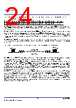
24 / 44 page  P9242-R3/RB Datasheet © 2019 Integrated Device Technology, Inc. 24 May 17, 2019 Figure 24. Recommended Message Structure for the User Data Transfer from the P9242-R3 to the P9221-R3 for 8 Bytes of User Data Byte 1 Byte2 Byte 3 Byte 4 Byte 5 Byte 6 Byte 7 Byte 8 Byte 9 Byte 10 Header Data 0 Data 1 Data 2 Data 3 Data 4 Data 5 Data 6 Data 7 Checksum The P9242-R3 also has the flexibility to send the same data multiple times based on the setting in register 0800HEX bits [2:1]. For example, if register 0800HEX bits [2:1] are set to 01BIN, the P9242-R3 sends the data two times. It starts the second data transfer immediately after finishing the first data transfer. The external MCU on the transmitter should set Command register 0800HEX bit [0] to 1BIN to trigger the communication after loading the user data into the outgoing user data registers and setting the Command register 0800HEX bits [7:1] appropriately. After receiving the communication trigger from the control register, the P9242-R3 waits for the end of the next Control Error Packet (CEP; see section 10.6) and sends the data into the channel by modulating the operating frequency. Figure 25 shows the timing diagram for the user data transfer from the P9242-R3 to the P9221-R3. The P9221-R3 and P9242-R3 cannot both send data into the channel at the same time. If two devices send data into the channel at the same time, the data will be corrupted; therefore the MCUs on the transmitter and receiver must establish an algorithm to avoid conflicting messages on the channel. Figure 25. Timing Diagram for the User Data Transfer from the P9242-R3 to the P9221-R3 CEP Packet CEP Packet User Data (FSK) Total 22 bits The LOAD pin on the P9242-R3 helps the external MCU to synchronize the data upload into the outgoing user data registers. In the power transfer phase, the external MCU can load the data into the outgoing user data registers on the falling edge of the LOAD pin. The P9242-R3 will reset register 0800HEX bit 0 to 0BIN immediately after sending the data into the channel. The external MCU on the transmitter can periodically check bit 0 in the P9242-R3 register 0800HEX to get an acknowledgment of successful data transmission into the channel. When the external MCU on the transmitter loads more than 2 bytes of user data into the outgoing registers, the P9242-R3 will reset register 0800HEX bit 0 to 0BIN after sending all the bytes into the channel. The P9242-R3 gives the WPC standard communication packets priority over the user data packets. The user data packets have the lowest priority. Therefore during the load transients, the P9242-R3 might skip sending the user data packets and give priority to the WPC communication packets. The P9242-R3 transfers the data into the channel at 200bps; however, the channel is usually busy transmitting the WPC standard communication packets. There is a very small window in which the user data can be transferred. Typically in the power transfer phase, a CEP packet is sent every 150msec. In one second, there will be only 6 to 7 time slots in which the P9242-R3 can send a maximum of 2 bytes of user data in each slot. As a result the effective maximum data transfer rate achieved for transfers from the P9242-R3 to the P9221-R3 is 110bps. The P9242-R3 does not wait for acknowledgement from the P9221-R3 or keep track of successful delivery of the data to the P9221-R3. The P9242-R3 only acts as a messenger and relies upon the external MCU on the receiver and transmitter to craft a lossless communication protocol by adding intelligence into the data they are transferring. |
|
链接网址 |
| ALLDATASHEET是否为您带来帮助? [ DONATE ] |
关于 Alldatasheet | 广告服务 | 联系我们 | 隐私政策 | 数据表链接 | 链接交换 | 制造商名单 All Rights Reserved©Alldatasheet.com |
| Russian : Alldatasheetru.com | Korean : Alldatasheet.co.kr | Spanish : Alldatasheet.es | French : Alldatasheet.fr | Italian : Alldatasheetit.com Portuguese : Alldatasheetpt.com | Polish : Alldatasheet.pl | Vietnamese : Alldatasheet.vn Indian : Alldatasheet.in | Mexican : Alldatasheet.com.mx | British : Alldatasheet.co.uk | New Zealand : Alldatasheet.co.nz |
|
Family Site : ic2ic.com |
icmetro.com |
 Chinese ▼
 English
 Chinese
 German
 Japanese
 Russian
 Korean
 Spanish
 French
 Italian
 Portuguese
 Polish
 Vietnamese
 Indian
 Mexican
 British
 New Zealand