|
数据搜索系统,热门电子元器件搜索 |
|
|
数据搜索系统,热门电子元器件搜索 |
|
P9242-R3 数据表(PDF) 26 Page - Renesas Technology Corp |
|
|
|||||||||||||||||||||||||||||
P9242-R3 数据表(HTML) 26 Page - Renesas Technology Corp |
|
|
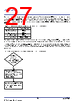
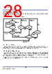
26 / 44 page  P9242-R3/RB Datasheet © 2019 Integrated Device Technology, Inc. 26 May 17, 2019 Figure 27. State Diagram for User Data Transmission from the P9242-R3 to the P9221-R3 Is P9242-R3 in the power transfer phase (register 06E0HEX = 09HEX)? Load outgoing user data registers (registers 0805HEX to 080EHEX) and set the number of bytes to be transferred in bits [6:3] in register 0800HEX accordingly Is the communication channel free (bit 0 of register 0800HEX = “0”) Yes Yes Set bit 0 of register 0800HEX to “1” to trigger the communication The P9242-R3 will reset bit 0 of register 0800HEX to “0” after sending the data into the channel 9.2 Reading Data Sent from the P9221-R3 The 9242-R3 can receive 8 bytes of information at a time. When the P9242-R3 receives data from the P9221-R3, it will generate an interrupt to the external MCU on the transmitter by pulling down the interrupt pin. The MCU can respond to the interrupt and read the data received flag in register 0801HEX bit 0 to confirm that the interrupt is generated because of the new incoming data. The Data_Received_Flag (register 0801HEX bit [0]) is set to 1BIN when there is new incoming data. |
|
链接网址 |
| ALLDATASHEET是否为您带来帮助? [ DONATE ] |
关于 Alldatasheet | 广告服务 | 联系我们 | 隐私政策 | 数据表链接 | 链接交换 | 制造商名单 All Rights Reserved©Alldatasheet.com |
| Russian : Alldatasheetru.com | Korean : Alldatasheet.co.kr | Spanish : Alldatasheet.es | French : Alldatasheet.fr | Italian : Alldatasheetit.com Portuguese : Alldatasheetpt.com | Polish : Alldatasheet.pl | Vietnamese : Alldatasheet.vn Indian : Alldatasheet.in | Mexican : Alldatasheet.com.mx | British : Alldatasheet.co.uk | New Zealand : Alldatasheet.co.nz |
|
Family Site : ic2ic.com |
icmetro.com |
 Chinese ▼
 English
 Chinese
 German
 Japanese
 Russian
 Korean
 Spanish
 French
 Italian
 Portuguese
 Polish
 Vietnamese
 Indian
 Mexican
 British
 New Zealand