|
数据搜索系统,热门电子元器件搜索 |
|
|
数据搜索系统,热门电子元器件搜索 |
|
AD8330ACP-R2 数据表(PDF) 14 Page - Analog Devices |
|
|
|||||||||||||||||||||||||||||
AD8330ACP-R2 数据表(HTML) 14 Page - Analog Devices |
|
|
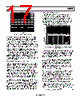
14 / 32 page  AD8330 Rev. C | Page 14 of 32 THEORY OF OPERATION CIRCUIT DESCRIPTION Many monolithic variable gain amplifiers use techniques that share common principles that are broadly classified as trans- linear. This term refers to circuit cells whose functions depend directly on the very predictable properties of bipolar junction transistors, notably the linear dependence of their transcon- ductance on collector current. Since the discovery of these cells in 1967, and their commercial exploitation in products developed during the early 1970s, accurate wide bandwidth analog multipliers, dividers, and variable gain amplifiers have invariably employed translinear principles. Although these techniques are well understood, the realization of a high performance variable gain amplifier (VGA) requires special technologies and attention to many subtle details in its design. The AD8330 is fabricated on a proprietary silicon- on-insulator, complementary bipolar IC process and draws on decades of experience in developing many leading edge products using translinear principles to provide an unprecedented level of versatility. Figure 45 shows a basic representative cell comprising just four transistors. This, or a very closely related form, is at the heart of most translinear multipliers, dividers, and VGAs. The key concepts are as follows: First, the ratio of the currents in the left-hand and right-hand pairs of transistors is identical, rep- resented by the modulation factor, x, with values between −1 and +1. Second, the input signal is arranged to modulate the fixed tail current, ID, to cause the variable value of x, introduced in the left-hand pair, to be replicated in the right-hand pair, and, thus, generate the output by modulating its nominally fixed tail current, IN. Third, the current gain of this cell is exactly G = IN/ID over many decades of variable bias current. In practice, the realization of the full potential of this circuit involves many other factors, but these three elementary ideas remain essential. By varying IN, the overall function is that of a two-quadrant analog multiplier, exhibiting a linear relationship to both the signal modulation factor (x) and this numerator current. On the other hand, by varying ID, a two-quadrant analog divider is realized, having a hyperbolic gain function with respect to the input factor, x, controlled by this denominator current. The AD8330 exploits both modes of operation. However, since a hyperbolic gain function is generally of less value than one in which the decibel gain is a linear function of a control input, a special interface is included to provide either increasing or decreasing exponential control of ID. INPUT IS xlD DENOMINATOR BIAS CURRENT ID Q1 Q2 Q4 Q3 (1–x) ID 2 +– LOOP AMPLIFIER (1–x) IN 2 NUMERATOR BIAS CURRENT IN OUTPUT IS xlN G = IN/ID (1+x) IN 2 (1–x) ID 2 Figure 45. Basic Core COMM OPHI INLO OPLO INHI VPSI VPSO CMOP MODE VDBS CMGN VMAG OFST R T N C L B N EVPOS BIAS AND VREF GAIN INTERFACE CM MODE AND OFFSET CONTROL OUTPUT STAGES OUTPUT CONTROL VGA CORE AD8330 Figure 46. Block Schematic Overall Structure Figure 46 shows a block schematic of the AD8330 locating the key sections. More detailed descriptions of its structure and features are provided throughout the Theory of Operation section; however, Figure 46 provides a general overview of its capabilities. The VGA core contains a more elaborate version of the cell shown in Figure 45. The current, ID, is controlled exponentially (linear-in-decibels) through the decibel gain interface at Pin VDBS and its local common, Pin CMGN. The gain span (that is, the decibel difference between maximum and minimum values) provided by this control function is slightly more than 50 dB. The absolute gain from input to output is a function of source and load impedance, and also depends on the voltage on a second gain control pin (VMAG), explained in the Normal Operating Conditions section. Normal Operating Conditions To minimize confusion, normal operating conditions are defined as follows: • The input pins are voltage driven (the source impedance is assumed to be zero); • The output pins are open circuited (the load impedance is assumed to be infinite); |
|
链接网址 |
| ALLDATASHEET是否为您带来帮助? [ DONATE ] |
关于 Alldatasheet | 广告服务 | 联系我们 | 隐私政策 | 数据表链接 | 链接交换 | 制造商名单 All Rights Reserved©Alldatasheet.com |
| Russian : Alldatasheetru.com | Korean : Alldatasheet.co.kr | Spanish : Alldatasheet.es | French : Alldatasheet.fr | Italian : Alldatasheetit.com Portuguese : Alldatasheetpt.com | Polish : Alldatasheet.pl | Vietnamese : Alldatasheet.vn Indian : Alldatasheet.in | Mexican : Alldatasheet.com.mx | British : Alldatasheet.co.uk | New Zealand : Alldatasheet.co.nz |
|
Family Site : ic2ic.com |
icmetro.com |
 Chinese ▼
 English
 Chinese
 German
 Japanese
 Russian
 Korean
 Spanish
 French
 Italian
 Portuguese
 Polish
 Vietnamese
 Indian
 Mexican
 British
 New Zealand