|
数据搜索系统,热门电子元器件搜索 |
|
|
数据搜索系统,热门电子元器件搜索 |
|
AD8330ACP-R2 数据表(PDF) 19 Page - Analog Devices |
|
|
|||||||||||||||||||||||||||||
AD8330ACP-R2 数据表(HTML) 19 Page - Analog Devices |
|
|
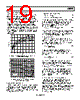
19 / 32 page  AD8330 Rev. C | Page 19 of 32 Input Common-Mode Range and Rejection Ratio Input Pin INHI and Pin INLO should be ac-coupled in most applications to achieve the stated noise performance. When direct coupling is used, care must be taken in setting the dc voltage level at these inputs, in general, and particularly when minimizing noise is critical. This objective is complicated by the fact that the common-mode level varies with the basic gain voltage, VDBS. Figure 55 shows this relationship for a supply voltage of 5 V, for temperatures of −40°C, +25°C, and +85°C. Figure 56 shows the input noise spectral density (RS = 0) vs. the input common-mode voltage, for VDBS = 0.5 V, 0.6 V, 0.75 V, and 1.5 V. It is apparent that there is a broad range over which the noise is unaffected by this dc level. The input CMRR is excellent (see Figure 16). VDBS (V) 0 2.6 3.2 3.1 3.0 2.9 2.8 2.7 0.2 0.4 0.6 0.8 1.0 1.2 1.4 1.6 T = +25°C T = +85°C T = –40°C Figure 55. Common-Mode Voltage at Input Pins vs. VDBS, for VS = 5 V, T = −40°C, + 25°C, and + 85°C COMMON-MODE VOLTAGE AT INHI, INLO (V) 0 26 22 20 18 16 14 12 10 8 4 6 24 0.4 0.8 1.2 1.6 2.0 2.4 2.8 3.2 3.6 4.0 4.4 4.8 VDBS = 1.5V VDBS = 0.75V VDBS = 0.6V VDBS = 0.5V SIMULATION Figure 56. Input Noise vs. Common-Mode Input Voltage for VDBS = 0.5 V, 0.6 V, 0.75 V, and 1.5 V Output Noise and Peak Swing The output noise of the AD8330 is the input noise multiplied by the overall gain, including any optional change to the voltage, VMAG, applied to Pin VMAG. The peak output swing is also proportional to this voltage, which, at low gains and high values of VMAG, affects the output noise. The scaling for VDBS = 0 is as follows: VOUT_PK = ±4 VMAG (8) VNOISE_OUT = (85 + 70 VMAG) nV/√Hz (9) For example, using a reduced value of VMAG = 0.25 V that lowers all gain values by 6 dB, the peak output swing is ±1 V (differ entially) and the output noise spectral density evaluates to 102.5 nV/√Hz. The peak output swing is no different at full gain, but the noise becomes VNOISE_OUT = (0.1 + 0.32 VMAG) μV/√Hz (10) for RS = 0 and VDBS = 1.5 V, assuming an input noise of 5 nV/√Hz. The output noise for very small values of VMAG (at or below 15 mV) is not precise, partly because the small input offset associated with this interface has a large effect on the gain. Offset Compensation The AD8330 includes an offset compensation feature that is operational in the default condition (no connection to Pin OFST). This loop introduces a high-pass filter function into the signal path, whose −3 dB corner frequency is at ( ) HP INT HPF C R f π = 2 1 (11) where CHP is the external capacitance added from OFST to CNTR, and RINT is an internal resistance of approximately 480 Ω, having a maximum uncertainty of about ±20%. This evaluates to HP HPF C f μ = 330 (CHP in μF) (12) A small amount of peaking at this corner when using small capacitor values can be avoided by adding a series resistor. Useful combinations are CHP = 3 nF, RHP = 180 Ω , f = 100 kHz; CHP = 33 nF, RHP = 10 Ω, f = 10 kHz; CHP = 0.33 μF, RHP = 0 Ω, f = 1 kHz; CHP = 3.3 μF, RHP = 0 Ω, f = 100 Hz. The offset compensation feature can be disabled simply by grounding the OFST pin. This provides a dc-coupled signal path, with no other effects on the overall ac response. Input offsets must be externally nulled in this mode of operation, as shown in Figure 58. Effects of Loading on Gain and AC Response The differential output impedance (RO) is 150 Ω, and the frequency response of the output stage is optimized for operation with a certain load capacitance on each output pin (OPHI and OPLO) to ground, in combination with a load resistance (RL) directly across these pins. In the absence of these capacitances, there is a small amount of peaking at the top extremity of the ac response. Suitable combinations are: RL = ∞, CL = 12 pF; RL = 150 Ω, CL = 25 pF; RL = 75 Ω, CL = 40 pF; RL = 50 Ω, CL = 50 pF. |
|
链接网址 |
| ALLDATASHEET是否为您带来帮助? [ DONATE ] |
关于 Alldatasheet | 广告服务 | 联系我们 | 隐私政策 | 数据表链接 | 链接交换 | 制造商名单 All Rights Reserved©Alldatasheet.com |
| Russian : Alldatasheetru.com | Korean : Alldatasheet.co.kr | Spanish : Alldatasheet.es | French : Alldatasheet.fr | Italian : Alldatasheetit.com Portuguese : Alldatasheetpt.com | Polish : Alldatasheet.pl | Vietnamese : Alldatasheet.vn Indian : Alldatasheet.in | Mexican : Alldatasheet.com.mx | British : Alldatasheet.co.uk | New Zealand : Alldatasheet.co.nz |
|
Family Site : ic2ic.com |
icmetro.com |
 Chinese ▼
 English
 Chinese
 German
 Japanese
 Russian
 Korean
 Spanish
 French
 Italian
 Portuguese
 Polish
 Vietnamese
 Indian
 Mexican
 British
 New Zealand