|
数据搜索系统,热门电子元器件搜索 |
|
|
数据搜索系统,热门电子元器件搜索 |
|
AD8330ACP-R2 数据表(PDF) 16 Page - Analog Devices |
|
|
|||||||||||||||||||||||||||||
AD8330ACP-R2 数据表(HTML) 16 Page - Analog Devices |
|
|
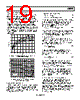
16 / 32 page  AD8330 Rev. C | Page 16 of 32 The gain can be increased or decreased by changing the voltage, VMAG, applied to the VMAG pin. The internally set default value of 500 mV is derived from the same band gap reference that determines the decibel scaling. The tolerance on this voltage, and mismatches in certain on-chip resistors, cause small gain errors (see the Specifications section). Though not all appli- cations of VGAs demand accurate gain calibration, it is a valuable asset in many situations, for example, in reducing design tolerances. Figure 47 shows the core circuit in more detail. The range and scaling of VDBS is independent of the supply voltage, and the Gain Control Pin VDBS presents a high incremental input re- sistance (~100 MΩ) with a low bias current (~100 nA), making the AD8330 easy to drive from a variety of gain control sources. Inversion of the Gain Slope The AD8330 supports many features that further extend the versatility of this VGA in wide bandwidth, gain control systems. For example, the Logic Pin MODE allows the slope of the gain function to be inverted, so that the basic gain starts at +50 dB for a gain voltage, VDBS, of zero and runs down to 0 dB when this voltage is at its maximum specified value of 1.5 V. The basic forms of these two gain control modes are shown in Figure 48. 0.25 10 20 VDBS (V) 0 30 40 50 0 0.50 0.75 1.0 1.25 1.50 MODE PIN LOW, GAIN DECREASES WITH VDBS MODE PIN HIGH, GAIN INCREASES WITH VDBS Figure 48. The Two Gain Directions of the AD8330 Gain Magnitude Control (VMAG) In addition to the basic linear-in-dB control, two more gain control features are provided. The voltage applied to Pin VMAG provides accurate linear-in-magnitude gain control with a very rapid response. The bandwidth of this interface is >100 MHz. When this pin is unconnected, VMAG assumes its default value of 500 mV (see Figure 47) to set up the basic 0 dB to 50 dB range. However, any voltage from ~15 mV to 5 V can be applied to either lower the gain by up to 30 dB or to raise it by 20 dB. The combined gain span is thus 100 dB, that is, the 50 dB basic gain span provided by VDBS plus a 60 dB linear-in-magnitude span provided by VMAG. The latter modifies the basic numerical gain GBN to generate a total gain, expressed here in magnitude terms V 5 . 0 MAG BN T V G G = (3) Using this to calculate the output voltage VOUT = 2 × GIN × VIN × VMAG (4) from which it is apparent that the AD8330 implements a linear, two-quadrant multiplier with a bipolar VIN and a unipolar VMAG. Because the AD8330 is a dc-coupled system, it can be used in many applications where a wideband two-quadrant multiplier function is required, from dc up to about 100 MHz from either input (VIN or VMAG). As VMAG is varied, so also is the peak output magnitude, up to a point where this is limited by the absolute output limit imposed by the supply voltage. In the absence of the latter effect, the peak output into an open circuited load is just VOUT_PK = ±4 VMAG (5) whereas for a load resistance of RL directly across OPHI and OPLO, it is ( ) 150 2 _ + ± = L L MAG PK OUT R R V V (6) These capabilities are illustrated in Figure 49, where VS = 6 V, RL = O/C, VDBS = 0 V, VIN is swept from −2.5 V dc to +2.5 V dc, and VMAG is set to 0.25 V, 0.5 V, 1 V, and 2 V. Except for the last value of VMAG, the peak output follows Equation 5. This exceeds the supply-limited value when VMAG = 2 V and the peak output is ±5.65 V, that is, ±6 V − 0.35 V. Figure 50 demonstrates the high speed multiplication capability. The signal input is a 100 MHz, 0.1 V sine wave, VDBS is set to 0.6 V, and VMAG is a square wave at 5 MHz alternating from 0.25 V to 1 V. The output is ideally a sine wave switching in amplitude between 0.5 V and 2 V. VIN ( V) 8 3 1 2 – 3 – 4 0 –4 –8 –1 6 2 –2 –6 02 VMAG = 2V 1V 0.5V 0.25V Figure 49. Effect of VMAG on Gain and Peak Output |
|
链接网址 |
| ALLDATASHEET是否为您带来帮助? [ DONATE ] |
关于 Alldatasheet | 广告服务 | 联系我们 | 隐私政策 | 数据表链接 | 链接交换 | 制造商名单 All Rights Reserved©Alldatasheet.com |
| Russian : Alldatasheetru.com | Korean : Alldatasheet.co.kr | Spanish : Alldatasheet.es | French : Alldatasheet.fr | Italian : Alldatasheetit.com Portuguese : Alldatasheetpt.com | Polish : Alldatasheet.pl | Vietnamese : Alldatasheet.vn Indian : Alldatasheet.in | Mexican : Alldatasheet.com.mx | British : Alldatasheet.co.uk | New Zealand : Alldatasheet.co.nz |
|
Family Site : ic2ic.com |
icmetro.com |
 Chinese ▼
 English
 Chinese
 German
 Japanese
 Russian
 Korean
 Spanish
 French
 Italian
 Portuguese
 Polish
 Vietnamese
 Indian
 Mexican
 British
 New Zealand