|
数据搜索系统,热门电子元器件搜索 |
|
|
数据搜索系统,热门电子元器件搜索 |
|
AD8330ACP-R2 数据表(PDF) 21 Page - Analog Devices |
|
|
|||||||||||||||||||||||||||||
AD8330ACP-R2 数据表(HTML) 21 Page - Analog Devices |
|
|
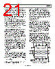
21 / 32 page  AD8330 Rev. C | Page 21 of 32 Connections to the input and output pins are not shown in Figure 57 because of the many options that are available. When the AD8330 is used to drive an ADC, connect the OPHI and OPLO pins directly to the differential inputs of a suitable converter, such as an AD9214. If an adjustment is needed to this common- mode level, it can be introduced by applying that voltage to the CNTR pin, or, more simply, by using a resistor from this pin to either ground or the supply (see the Applications section). The CNTR pin can also supply the common-mode voltage to an ADC that supports such a feature. When the loads to be driven introduce a dc resistive path to ground, coupling capacitors must be used. These should be of sufficient value to pass the lowest frequency components of the signal without excessive attenuation. Keep in mind that the voltage swing on such loads alternate both above and below ground, requiring that the subsequent component must be able to cope with negative signal excursions. Gain and Swing Adjustments When Loaded The output can also be coupled to a load via a transformer to achieve a higher load power by impedance transformation. For example, using a 2:1 turns ratio, a 50 Ω final load presents a 200 Ω load on the output. The gain loss (relative to the basic value with no termination) is 20 log10{(200+150)/200} or 4.86 dB, which can be restored by raising the voltage on the VMAG pin by a factor of 104.86/20 or × 1.75, from its basic value of 0.5 V to 0.875 V. This also restores the peak swing at the 200 Ω level to ±2 V, or ±1 V into the 50 Ω final load. Whenever a stable supply voltage is available, additional voltage swing can be provided by adding a resistor from the VMAG pin to the supply. The calculation is based on knowing that the in- ternal bias is delivered via a 5 kΩ source; because an additional 0.375 V is needed, the current in this external resistor must be 0.375 V/5 kΩ = 75 μA. Thus, using a 5 V supply, a resistor of 5 V − 0.875 V/75 μA = 55 kΩ is used. Based on this example, the corrections for other load conditions are easy to calculate. If the effects on gain and peak output swing due to supply variations cannot be tolerated, VMAG must be driven by an accurate voltage. Input Coupling The dc common-mode voltage at the input pins varies with the supply, the basic gain bias, and temperature (see Figure 55); for this reason, many applications need to use coupling capaci- tors from the source that are large enough to support the lowest frequencies to be transmitted. Using one capacitor at each input pin, their minimum values can be readily found from the expression HPF IN_CPL f C μF 320 = (15) where fHPF is the –3dB frequency expressed in hertz. Thus, for an fHPF of 10 kHz, 33 nF capacitors are used. Occasionally, it is possible to avoid the use of coupling capacitors when the dc level of the driving source is within a certain range, as shown in Figure 56. This range extends from 3.5 V to 4.5 V when using a 5 V supply, and at high basic gains, where the effect of an incorrect dc level degrades the noise level due to internal aspects of the input stage. For example, suppose the driver, IC, is an LNA having an output topology in which its load resistors are taken to the supply, and the output is buffered by emitter followers. This presents a source for the AD8330 that can readily be directly coupled. DC-Coupled Signal Path In many cases, where the VGA is not required to provide its lowest noise, the full common-mode input range of zero to VS can be used without problems, avoiding the need for any ac coupling means. However, such direct coupling at both the input and output does not automatically result in a fully dc-coupled signal path. The internal offset compensation loop must also be disengaged by connecting the OFST pin to ground. Keep in mind that at the maximum basic gain of 50 dB (×316), every millivolt of offset at the input, arising from whatever source, causes an output offset of 316 mV, which is an appreciable fraction of the peak output swing. Since the offset correction loop is placed after the front-end variable gain sections of the AD8330, the most effective way of dealing with such offsets is at the input pins, as shown in Figure 58. For example, assume, for illustrative purposes, that the resistances associated with each side of the source in a cer- tain application are 50 Ω. If this source has a very low (op amp) output impedance, the extra resistors should be inserted, with a negligible noise penalty and an attenuation of only 0.83 dB. The resistor values shown provide a trim range of about ±2 mV. COMM OPHI INLO OPLO INHI VPSI VPSO CMOP MODE VDBS CMGN VMAG OFST R T N C L B N E VPOS BIAS AND V-REF GAIN INTERFACE CM MODE AND OFFSET CONTROL OUTPUT STAGES OUTPUT CONTROL VGA CORE OUTPUT, ±2V MAX NC BASIC GAIN BIAS VDBS: 0V TO 1.5V 1 D R CD1 CD3 RD2 50kΩ 75kΩ RS ASSUMED TO BE 50Ω ON EACH SIDE GROUND CD2 VS 2.7V TO 6V Figure 58. Input Offset Nulling in a DC-Coupled System |
|
链接网址 |
| ALLDATASHEET是否为您带来帮助? [ DONATE ] |
关于 Alldatasheet | 广告服务 | 联系我们 | 隐私政策 | 数据表链接 | 链接交换 | 制造商名单 All Rights Reserved©Alldatasheet.com |
| Russian : Alldatasheetru.com | Korean : Alldatasheet.co.kr | Spanish : Alldatasheet.es | French : Alldatasheet.fr | Italian : Alldatasheetit.com Portuguese : Alldatasheetpt.com | Polish : Alldatasheet.pl | Vietnamese : Alldatasheet.vn Indian : Alldatasheet.in | Mexican : Alldatasheet.com.mx | British : Alldatasheet.co.uk | New Zealand : Alldatasheet.co.nz |
|
Family Site : ic2ic.com |
icmetro.com |
 Chinese ▼
 English
 Chinese
 German
 Japanese
 Russian
 Korean
 Spanish
 French
 Italian
 Portuguese
 Polish
 Vietnamese
 Indian
 Mexican
 British
 New Zealand