|
数据搜索系统,热门电子元器件搜索 |
|
|
数据搜索系统,热门电子元器件搜索 |
|
SSM2211CP-R2 数据表(PDF) 17 Page - Analog Devices |
|
|
|||||||||||||||||||||||||||||
SSM2211CP-R2 数据表(HTML) 17 Page - Analog Devices |
|
|
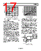
17 / 24 page  SSM2211 Rev. D | Page 17 of 24 OUTPUT POWER (W) 0.35 0.30 0 0 0.4 0.1 0.2 0.3 0.20 0.15 0.10 0.05 0.25 VDD = 5V RL = 4Ω RL = 8Ω RL = 16Ω Figure 45. Power Dissipation vs. Single-Ended Output Power with VDD = 5 V The maximum power dissipation for a single-ended output is L DD MAX DISS R V P 2 2 , π 2 = (11) OUTPUT VOLTAGE HEADROOM The outputs of both amplifiers in the SSM2211 can come to within 400 mV of either supply rail while driving an 8 Ω load. As compared to equivalent competitor products, the SSM2211 has a higher output voltage headroom. This means that the SSM2211 can deliver an equivalent maximum output power while running from a lower supply voltage. By running at a lower supply voltage, the internal power dissipation of the device is reduced, as can be seen in Equation 9. This extended output headroom, along with the LFCSP package, allows the SSM2211 to operate in higher ambient temperatures than competitor devices. The SSM2211 is also capable of providing amplification even at supply voltages as low as 2.7 V. The maximum power available at the output is a function of the supply voltage. Therefore, as the supply voltage decreases, so does the maximum power output from the device. The maximum output power vs. supply voltage at various bridge-tied load resistances is shown in Figure 46. The maximum output power is defined as the point at which the output has 1% total harmonic distortion (THD + N). To find the minimum supply voltage needed to achieve a specified maximum undistorted output power use Figure 46. For example, an application requires only 500 mW to be output for an 8 Ω speaker. With the speaker connected in a bridged-output configuration, the minimum supply voltage required is 3.3 V. SUPPLY VOLTAGE (V) 0 1.5 5.0 2.0 2.5 3.0 3.5 4.0 4.5 1.6 1.0 0.8 0.4 0.2 1.4 1.2 0.6 RL = 4 Ω RL = 8 Ω RL = 16 Ω Figure 46. Maximum Output Power vs. VSY Shutdown Feature The SSM2211 can be put into a low power consumption shut- down mode by connecting Pin 1 to 5 V. In shutdown mode, the SSM2211 has an extremely low supply current of less than 10 nA. This makes the SSM2211 ideal for battery-powered applications. Connect Pin 1 to ground for normal operation. Connecting Pin 1 to VDD mutes the outputs and puts the device into shutdown mode. A pull-up or pull-down resistor is not required. Pin 1 should always be connected to a fixed potential, either VDD or ground, and never be left floating. Leaving Pin 1 unconnected can produce unpredictable results. AUTOMATIC SHUTDOWN-SENSING CIRCUIT Figure 47 shows a circuit that can be used to take the SSM2211 in and out of shutdown mode automatically. This circuit can be set to turn the SSM2211 on when an input signal of a certain amplitude is detected. The circuit also puts the device into low power shutdown mode if an input signal is not sensed within a certain amount of time. This can be useful in a variety of portable radio applications, where power conservation is critical. SSM2211 VIN VDD C2 R5 R6 R1 R3 R2 D1 C1 R4 R7 4 VDD OP181 A2 1 5 R8 A1 – + VDD 8 NOTE ADDITIONAL PINS OMITTED FOR CLARITY Figure 47. Automatic Shutdown Circuit |
|
|
链接网址 |
| ALLDATASHEET是否为您带来帮助? [ DONATE ] |
关于 Alldatasheet | 广告服务 | 联系我们 | 隐私政策 | 数据表链接 | 链接交换 | 制造商名单 All Rights Reserved©Alldatasheet.com |
| Russian : Alldatasheetru.com | Korean : Alldatasheet.co.kr | Spanish : Alldatasheet.es | French : Alldatasheet.fr | Italian : Alldatasheetit.com Portuguese : Alldatasheetpt.com | Polish : Alldatasheet.pl | Vietnamese : Alldatasheet.vn Indian : Alldatasheet.in | Mexican : Alldatasheet.com.mx | British : Alldatasheet.co.uk | New Zealand : Alldatasheet.co.nz |
|
Family Site : ic2ic.com |
icmetro.com |
 Chinese ▼
 English
 Chinese
 German
 Japanese
 Russian
 Korean
 Spanish
 French
 Italian
 Portuguese
 Polish
 Vietnamese
 Indian
 Mexican
 British
 New Zealand