|
数据搜索系统,热门电子元器件搜索 |
|
|
数据搜索系统,热门电子元器件搜索 |
|
SSM2211CP-R2 数据表(PDF) 20 Page - Analog Devices |
|
|
|||||||||||||||||||||||||||||
SSM2211CP-R2 数据表(HTML) 20 Page - Analog Devices |
|
|
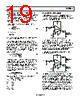
20 / 24 page  SSM2211 Rev. D | Page 20 of 24 The polarity of the speakers is important, as each output is 180 degrees out of phase with the other. By connecting the minus terminal of Speaker 1 to Pin 5, and the plus terminal of Speaker 2 to Pin 8, proper speaker phase can be established. Therefore, for PO = 1 W and RL = 8 Ω, V = 2.8 V rms, or 8 V pp. If the available input signal is 1.4 V rms or more, use the board as is, with RF = RI = 20 kΩ. If more gain is needed, increase the value of RF. When you have determined the closed-loop gain required by your source level, and can develop 1 W across the 8 Ω load resistor with the normal input signal level, replace the resistor with your speaker. Your speaker can be connected across the VO1 and VO2 posts for bridged-mode operation only after the 8 Ω load resistor is removed. For no phase inversion, VO2 must be connected to the (+) terminal of the speaker. The maximum power dissipation of the device, assuming both loads are equal, can be found by doubling Equation 11. If the loads are different, use Equation 11 to find the power dissipa- tion caused by each load, then take the sum to find the total power dissipated by the SSM2211. EVALUATION BOARD An evaluation board for the SSM2211 is available. For more information, call 1-800-ANALOGD. 8 SSM2211 5 VO2 GND CH A CH B PROBES CH B INV. ON DISPLAY A+B OSCILLOSCOPE 2.5V COMMON MODE VO1 8 Ω 1W V+ 8 4 SSM2211 5 3 2 1 VO2 6 J1 J2 C1 0.1µF 7 CIN 1µF CW ON SHUTDOWN R1 51kΩ + + RI 20kΩ RF 20kΩ VO1 RL 1W 8Ω VOLUME 20kΩ POT. AUDIO INPUT C1 0.1µF C2 10µF Figure 51. Using an Oscilloscope to Display the Bridged-Output Voltage Figure 50. Evaluation Board Schematic The voltage gain of the SSM2211 is given by Equation 20. I F V R R A × = 2 (20) To use the SSM2211 in a single-ended-output configuration, replace J1 and J2 jumpers with electrolytic capacitors of a suitable value, with the negative terminals to the output terminals VO1 and VO2. The single-ended loads can then be returned to ground. Note that the maximum output power is reduced to 250 mW (one-quarter of the rated maximum), due to the maximum swing in the nonbridged mode being one-half and power being proportional to the square of the voltage. For frequency response down 3 dB at 100 Hz, a 200 μF capacitor is required with 8 Ω speakers. The SSM2211 evaluation board also comes with a shutdown switch, which allows the user to switch between on (normal operation) and the power-conserving shutdown mode. If desired, the input signal may be attenuated by turning the 10 kΩ potentiometer in the CW (clockwise) direction. CIN isolates the input common-mode voltage (VD/2) present at Pin 2 and Pin 3. With V+ = 5 V, there is 2.5 V common-mode voltage present at both output terminals, VO1 and VO2, as well. LFCSP PRINTED CIRCUIT BOARD LAYOUT CONSIDERATIONS The LFCSP is a plastic encapsulated package with a copper lead frame substrate. This is a leadless package with solder lands on the bottom surface of the package, instead of conventional formed perimeter leads. A key feature that allows the user to reach the quoted θJA performance is the exposed die attach paddle (DAP) on the bottom surface of the package. When soldered to the PCB, the DAP can provide efficient conduction of heat from the die to the PCB. In order to achieve optimum package performance, consideration should be given to the PCB pad design for both the solder lands and the DAP. For further information the user is directed to the Amkor Technology document, “Application Notes for Surface Mount Assembly of Amkor’s MicroLead Frame (MLF) Packages.” This can be downloaded from the Amkor Technology website, www.amkor.com, as a product application note. CAUTION: The ground lead of the oscilloscope probe, or any other instrument used to measure the output signal, must not be connected to either output, as this shorts out one of the amplifier outputs and can possibly damage the device. A safe method of displaying the differential output signal using a grounded scope is shown in Figure 51. Connect Channel A probe to the VO2 terminal post. Connect Channel B probe to the VO1 post. Invert Channel B, and add the two channels together. Most multichannel oscilloscopes have this feature built in. If you must connect the ground lead of the test instrument to either output signal pins, a power-line isolation transformer must be used to isolate the instrument ground from the power supply ground. Recall that R P V × = |
|
|
链接网址 |
| ALLDATASHEET是否为您带来帮助? [ DONATE ] |
关于 Alldatasheet | 广告服务 | 联系我们 | 隐私政策 | 数据表链接 | 链接交换 | 制造商名单 All Rights Reserved©Alldatasheet.com |
| Russian : Alldatasheetru.com | Korean : Alldatasheet.co.kr | Spanish : Alldatasheet.es | French : Alldatasheet.fr | Italian : Alldatasheetit.com Portuguese : Alldatasheetpt.com | Polish : Alldatasheet.pl | Vietnamese : Alldatasheet.vn Indian : Alldatasheet.in | Mexican : Alldatasheet.com.mx | British : Alldatasheet.co.uk | New Zealand : Alldatasheet.co.nz |
|
Family Site : ic2ic.com |
icmetro.com |
 Chinese ▼
 English
 Chinese
 German
 Japanese
 Russian
 Korean
 Spanish
 French
 Italian
 Portuguese
 Polish
 Vietnamese
 Indian
 Mexican
 British
 New Zealand