|
数据搜索系统,热门电子元器件搜索 |
|
|
数据搜索系统,热门电子元器件搜索 |
|
SSM2211CP-R2 数据表(PDF) 18 Page - Analog Devices |
|
|
|||||||||||||||||||||||||||||
SSM2211CP-R2 数据表(HTML) 18 Page - Analog Devices |
|
|
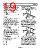
18 / 24 page  SSM2211 Rev. D | Page 18 of 24 The input signal to the SSM2211 is also connected to the non- inverting terminal of A2. R1, R2, and R3 set the threshold voltage at which the SSM2211 is to be taken out of shutdown mode. D1 half-wave rectifies the output of A2, discharging C1 to ground when an input signal greater than the set threshold voltage is detected. R4 controls the charge time of C1, which sets the time until the SSM2211 is put back into shutdown mode after the input signal is no longer detected. R5 and R6 are used to establish a voltage reference point equal to half of the supply voltage. R7 and R8 set the gain of the SSM2211. A 1N914 or equivalent diode is required for D1, and A2 must be a rail-to-rail output amplifier, such as OP181 or equivalent. This ensures that C1 discharges sufficiently to bring the SSM2211 out of shutdown mode. To find the appropriate component values, first, the gain of A2 must be determined by THS SY MIN V, V V A = (12) where: VSY is the single supply voltage. VTHS is the threshold voltage. AV must be set to a minimum of 2 for the circuit to work properly. Next, choose R1 and set R2 to ⎟⎟ ⎠ ⎞ ⎜⎜ ⎝ ⎛ − = V A R1 R2 2 1 (13) Find R3 as ( 1 − + × = V A R2 R2 R2 R1 R3 ) (14) C1 can be arbitrarily set but should be small enough to prevent A2 from becoming capacitively overloaded. R4 and C1 control the shutdown rate. To prevent intermittent shutdown with low frequency input signals, the minimum time constant must be LOW f C1 R4 10 ≥ × (15) where fLOW is the lowest input frequency expected. SHUTDOWN-CIRCUIT DESIGN EXAMPLE In this example, a portable radio application requires the SSM2211 to be turned on when an input signal greater than 50 mV is detected. The device needs to return to shutdown mode within 500 ms after the input signal is no longer detected. The lowest frequency of interest is 200 Hz, and a 5 V supply is used. The minimum gain of the shutdown circuit, from Equation 12, is AV = 100. R1 is set to 100 kΩ. Using Equation 13 and Equation 14, R2 = 98 kΩ and R3 = 4.9 MΩ. C1 is set to 0.01 μF, and based on Equation 15, R4 is set to 10 MΩ . To minimize power supply current, R5 and R6 are set to 10 MΩ. The previous procedure provides an adequate starting point for the shutdown circuit. Some component values may need to be adjusted empirically to optimize performance. START-UP POPPING NOISE During power-up or release from shutdown mode, the midrail bypass capacitor, CB, determines the rate at which the SSM2211 starts up. By adjusting the charging time constant of CB, the start-up pop noise can be pushed into the subaudible range, greatly reducing start-up popping noise. On power-up, the midrail bypass capacitor is charged through an effective resistance of 25 kΩ. To minimize start-up popping, the charging time constant for CB needs to be greater than the charging time constant for the input coupling capacitor, CC. CB × 25 kΩ > CC × R1 (16) For an application where R1 = 10 kΩ and CC = 0.22 μF, CB must be at least 0.1 μF to minimize start-up popping noise. SSM2211 Amplifier Design Example Maximum Output Power 1 W Input Impedance 20 kΩ Load Impedance 8 Ω Input Level 1 V rms Bandwidth 20 Hz − 20 kHz ± 0.25 dB The configuration shown in Figure 42 is used. The first thing to determine is the minimum supply rail necessary to obtain the specified maximum output power. From Figure 46, for 1 W of output power into an 8 Ω load, the supply voltage must be at least 4.6 V. A supply rail of 5 V can be easily obtained from a |
|
|
链接网址 |
| ALLDATASHEET是否为您带来帮助? [ DONATE ] |
关于 Alldatasheet | 广告服务 | 联系我们 | 隐私政策 | 数据表链接 | 链接交换 | 制造商名单 All Rights Reserved©Alldatasheet.com |
| Russian : Alldatasheetru.com | Korean : Alldatasheet.co.kr | Spanish : Alldatasheet.es | French : Alldatasheet.fr | Italian : Alldatasheetit.com Portuguese : Alldatasheetpt.com | Polish : Alldatasheet.pl | Vietnamese : Alldatasheet.vn Indian : Alldatasheet.in | Mexican : Alldatasheet.com.mx | British : Alldatasheet.co.uk | New Zealand : Alldatasheet.co.nz |
|
Family Site : ic2ic.com |
icmetro.com |
 Chinese ▼
 English
 Chinese
 German
 Japanese
 Russian
 Korean
 Spanish
 French
 Italian
 Portuguese
 Polish
 Vietnamese
 Indian
 Mexican
 British
 New Zealand