|
数据搜索系统,热门电子元器件搜索 |
|
|
数据搜索系统,热门电子元器件搜索 |
|
RT8800AGQV 数据表(PDF) 14 Page - Richtek Technology Corporation |
|
|
|||||||||||||||||||||||||||||
RT8800AGQV 数据表(HTML) 14 Page - Richtek Technology Corporation |
|
|
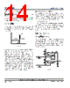
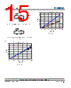
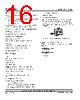
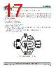
14 / 21 page  RT8800A 14 DS8800A-04 August 2007 www.richtek.com All brand name or trademark belong to their owner respectively Rewriting Equation (3), we get CSN LX LX_Valley COMM F R R I R V ≥ × × The technique mentioned above also provides output voltage offset function specified by Intel ® VRD10.x. The offset voltage level is calculated as: F CSN ADJ OFFSET V R R V = Enough bias current is required for a Schottky to act like a voltage source. Users should choose the appropriate RCS based on the IV characteristic of the diode (Figure 12) Figure 12 I V Zone 1 Zone 2 IV Characteristic According to Figure 12, the forward voltage of diode will be different results from the different conduction current. So when the characteristic of diode in the circuit you design is in zone 1, this will result in Spec. mis-met. It is because when the VCORE is changed during DVID, the node VCORE- VF is also changed to produce the differential conduction current of diode ΔI and the ΔI will result in producing the differential forward voltage of diode ΔVF Referring to Equation (1). The ΔVF would get ΔIX. Then the VCORE must be subtracted the extra voltage V(EXT)( ΔIX x RADJ ) during DVID. So you will get the ΔVCORE = V(MAX) - V(MIN) - V(EXT) during DVID tests. In order to reduce the effect results from diode. The better choice is to decrease the Rcs to increase the conduction current of diode I to get better V characteristic of diode in Zone 2. Over Voltage Protection (OVP) The RT8800A continuously monitors voltage at FB pin. OVP is triggered if FB voltage is 500mV higher than the voltage at PI pin. RT8800A latches off and turns on lower MOSFET to protect the load from damage upon on OVP trip. It can only be reset by DVD and VDD pins. Current Ratio Setting Current ratio adjustment is possible as described below. It is important for achieving thermal balance in practical application where thermal conditions between phases are not identical. Figure 13 shows the application circuit of GM for current ratio requirement. According to Basic Circuit Theory, if LX LX PX SX PX X X PX SX LX X R I R R R V then C ) //R (R R L × × + = × = With other phase kept unchanged, this phase would share (RPX+RSX)/RPX times current than other phases. Figure 14 and 15 show different current ratio setting for the power stage when Phase 3 is programmed 2 times current than other phases. Figure 16 and 17 compare the above current ratio setting results. Figure 13 (4) T T LX RLX ILX VOUT RSX CX + VX - RPX |
|
|
链接网址 |
| ALLDATASHEET是否为您带来帮助? [ DONATE ] |
关于 Alldatasheet | 广告服务 | 联系我们 | 隐私政策 | 数据表链接 | 链接交换 | 制造商名单 All Rights Reserved©Alldatasheet.com |
| Russian : Alldatasheetru.com | Korean : Alldatasheet.co.kr | Spanish : Alldatasheet.es | French : Alldatasheet.fr | Italian : Alldatasheetit.com Portuguese : Alldatasheetpt.com | Polish : Alldatasheet.pl | Vietnamese : Alldatasheet.vn Indian : Alldatasheet.in | Mexican : Alldatasheet.com.mx | British : Alldatasheet.co.uk | New Zealand : Alldatasheet.co.nz |
|
Family Site : ic2ic.com |
icmetro.com |
 Chinese ▼
 English
 Chinese
 German
 Japanese
 Russian
 Korean
 Spanish
 French
 Italian
 Portuguese
 Polish
 Vietnamese
 Indian
 Mexican
 British
 New Zealand