|
数据搜索系统,热门电子元器件搜索 |
|
|
数据搜索系统,热门电子元器件搜索 |
|
RT8800AGQV 数据表(PDF) 17 Page - Richtek Technology Corporation |
|
|
|||||||||||||||||||||||||||||
RT8800AGQV 数据表(HTML) 17 Page - Richtek Technology Corporation |
|
|
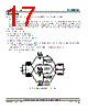
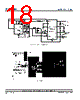
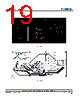
17 / 21 page  RT8800A 17 DS8800A-04 August 2007 www.richtek.com All brand name or trademark belong to their owner respectively Layout Guide Place the high-power switching components first, and separate them from sensitive nodes. 1. Most critical path: The current sense circuit is the most sensitive part of the converter. The current sense resistors tied to ISP1,2,3 and ICOMMON should be located not more than 0.5 inch from the IC and away from the noise switching nodes. The PCB trace of sense nodes should be parallel and as short as possible. R&C filter of choke should place close to PWM and the R & C connect directly to the pin of each output choke, use 10 mil differencial pair, and 20 mil gap to other phase pair. Less via as possible. 2. Switching ripple current path: a. Input capacitor to high side MOSFET. b. Low side MOSFET to output capacitor. c. The return path of input and output capacitor. d. Separate the power and signal GND. e. The switching nodes (the connection node of high/low side MOSFET and inductor) is the most noisy points.Keep them away from sensitive small-signal node. f . Reduce parasitic R, L by minimum length, enough copper thickness and avoiding of via. 3. MOSFET driver should be closed to MOSFET. Figure 18. Power Stage Ripple Current Path SW2 L2 SW1 L1 C OUT R L V OUT V IN R IN C IN V |
|
|
链接网址 |
| ALLDATASHEET是否为您带来帮助? [ DONATE ] |
关于 Alldatasheet | 广告服务 | 联系我们 | 隐私政策 | 数据表链接 | 链接交换 | 制造商名单 All Rights Reserved©Alldatasheet.com |
| Russian : Alldatasheetru.com | Korean : Alldatasheet.co.kr | Spanish : Alldatasheet.es | French : Alldatasheet.fr | Italian : Alldatasheetit.com Portuguese : Alldatasheetpt.com | Polish : Alldatasheet.pl | Vietnamese : Alldatasheet.vn Indian : Alldatasheet.in | Mexican : Alldatasheet.com.mx | British : Alldatasheet.co.uk | New Zealand : Alldatasheet.co.nz |
|
Family Site : ic2ic.com |
icmetro.com |
 Chinese ▼
 English
 Chinese
 German
 Japanese
 Russian
 Korean
 Spanish
 French
 Italian
 Portuguese
 Polish
 Vietnamese
 Indian
 Mexican
 British
 New Zealand