|
数据搜索系统,热门电子元器件搜索 |
|
|
数据搜索系统,热门电子元器件搜索 |
|
AD7450ARM 数据表(PDF) 12 Page - Analog Devices |
|
|
|||||||||||||||||||||||||||||
AD7450ARM 数据表(HTML) 12 Page - Analog Devices |
|
|
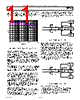
12 / 24 page  REV. PrJ PRELIMINARY TECHNICAL DATA –12– AD7450 100...000 +VREF -1LSB 100...001 100...010 111...111 000...000 000...001 011...110 011...111 -VREF +1LSB 0LSB 1LSB = 2xVREF/4096 ANALOG INPUT (VIN+-VIN-) Figure 5. AD7450 Ideal Transfer Characteristic TYPICAL CONNECTION DIAGRAM Figure 6 shows a typical connection diagram for the AD7450 for both 5 V and 3 V supplies. In this setup the GND pin is connected to the analog ground plane of the system. The VREF pin is connected to either a 2.5 V or a 1.25 V decoupled reference source depending on the power supply, to set up the analog input range. The com- mon mode voltage has to be set up externally and is the value that the two inputs are centered on. For more details on driving the differential inputs and setting up the com- mon mode, see the ‘Driving Differential Inputs’ section. The conversion result for the ADC is output in a 16-bit word consisting of four leading zeros followed by the MSB of the 12-bit result. For applications where power consumption is of concern, the power-down mode should be used between conversions or bursts of several conver- sions to improve power performance. See ‘Modes of Operation’ section. CM* CM* * CM - COMMON MODE VOLTAGE VIN+ VIN- VDD SCLK SDATA CS GND VREF µC/µP SERIAL INTERFACE +3V/+5V SUPPLY 1.25V/2.5V VREF 0.1µF 0.1µF 10µF AD7450 VREF P-to-P VREF P-to-P Figure 6. Typical Connection Diagram THE ANALOG INPUT The analog input of the AD7450 is fully differential. Dif- ferential signals have a number of benefits over single ended signals including noise immunity based on the device’s common mode rejection, improvements in distor- tion performance, doubling of the device’s available dynamic range and flexibility in input ranges and bias points. Figure 7 defines the fully differential analog input of the AD7450. VIN+ AD7450 VIN- VREF P-to-P VREF P-to-P COMMON MODE VOLTAGE Figure 7. Differential Input Definition The amplitude of the differential signal is the difference between the signals applied to the VIN+ and VIN- pins (i.e. VIN+ - VIN-). VIN+ and VIN- are simultaneously driven by two signals each of amplitude VREF that are 180° out of phase. The amplitude of the differential signal is therefore -VREF to +VREF peak-to-peak (i.e. 2 x VREF). This is re- gardless of the common mode (CM). The common mode is the average of the two signals, i.e. (VIN+ + VIN-)/2 and is therefore the voltage that the two inputs are centered on. This results in the span of each input being CM ± VREF/2. This voltage has to be set up externally and its range var- ies with VREF. As the value of VREF increases, the common mode range decreases. When driving the inputs with an amplfier, the actual common mode range will be determined by the amplifier’s output voltage swing. Figure 8 shows how the common mode range varies with VREF for a 5 V power supply and figure 9 shows an ex- ample of the common mode range when using the AD8138 differential amplifer to drive the analog inputs. The common mode must be in this range to guarantee the specifications. With a 3V power supply, the Common Mode range is TBD. For ease of use, the common mode can be set up to be equal to VREF, resulting in the differential signal being ±VREF centered on VREF. When a conversion takes place, the common mode is rejected resulting in a virtually noise free signal of amplitude -VREF to +VREF corresponding to he digital codes of 0 to 4095. |
|
|
链接网址 |
| ALLDATASHEET是否为您带来帮助? [ DONATE ] |
关于 Alldatasheet | 广告服务 | 联系我们 | 隐私政策 | 数据表链接 | 链接交换 | 制造商名单 All Rights Reserved©Alldatasheet.com |
| Russian : Alldatasheetru.com | Korean : Alldatasheet.co.kr | Spanish : Alldatasheet.es | French : Alldatasheet.fr | Italian : Alldatasheetit.com Portuguese : Alldatasheetpt.com | Polish : Alldatasheet.pl | Vietnamese : Alldatasheet.vn Indian : Alldatasheet.in | Mexican : Alldatasheet.com.mx | British : Alldatasheet.co.uk | New Zealand : Alldatasheet.co.nz |
|
Family Site : ic2ic.com |
icmetro.com |
 Chinese ▼
 English
 Chinese
 German
 Japanese
 Russian
 Korean
 Spanish
 French
 Italian
 Portuguese
 Polish
 Vietnamese
 Indian
 Mexican
 British
 New Zealand