|
数据搜索系统,热门电子元器件搜索 |
|
|
数据搜索系统,热门电子元器件搜索 |
|
AD7450ARM 数据表(PDF) 15 Page - Analog Devices |
|
|
|||||||||||||||||||||||||||||
AD7450ARM 数据表(HTML) 15 Page - Analog Devices |
|
|
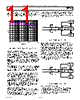
15 / 24 page  REV. PrJ PRELIMINARY TECHNICAL DATA –15– AD7450 The AD8138 is specified with 3 V, 5 V and ±5 V power supplies but the best results are obtained when it is supplied by ±5 V. A lower cost device that could also be used in this configuration with slight differences in characteristics to the AD8138 but with similar performance and operation is the AD8132. 2.5V 3.75V 1.25V Rs* Rs* Rf2 2.5V 3.75V 1.25V EXTERNAL VREF (2.5V) VREF VIN+ AD7450 VIN- AD8138 C* C* *Moun t as close to the AD7450 as possible and ensure high precision Rs and Cs are used Rs - 10R; C - 1nF; Rg1=Rf1=Rf2= 499R; Rg2 = 523R Rf1 Rg1 Vocm 51R Rg2 . GND +2.5V -2.5V Figure 14. Using the AD8138 as a Single Ended to Differen- tial Amplifier Opamp Pair An opamp pair can be used to directly couple a differential signal to the AD7450. The circuit configurations shown in figures 15(a) and 15(b) show how a dual opamp can be used to convert a single ended signal into a differential signal for both a bipolar and a unipolar input signal re- spectively. The voltage applied to point A is the Common Mode Voltage. In both diagrams, it is connected in some way to the reference but any value in the common mode range can be input here to setup the common mode. Examples of suitable dual opamps that could be used in this configura- tion to provide differential drive to the AD7450 are the AD8042, AD8056 and the AD8022. Care must be taken when chosing the opamp used, as the selection will depend on the required power supply and the system performance objectives. The driver circuits in fig- ures 15(a) and 15(b) are optimized for dc coupling applications requiring optimum distortion performance. The differential op-amp driver circuit in figure 15(a) is configured to convert and level shift a 2.5 V p-p single ended, ground referenced (bipolar) signal to a 5 V p-p differential signal centered at the VREF level of the ADC. The circuit configuration shown in figure 15(b) converts a unipolar, single ended signal into a differential signal. GND VREF P-to-P 27 27 390 220 220 10K EXTERNAL VREF 220 VDD V+ V+ V- V- VIN+ VIN- VREF AD7450 220 20K . 0.1µF . . A Figure 15(a). Dual Opamp Circuit to Convert a Single Ended Bipolar Input into a Differential Input GND VREF P-to-P 27 27 390 220 10K EXTERNAL VREF 220 VDD V+ V+ V- V- VIN+ VIN- VREF AD7450 220 . . 0.1µF A VREF/2 Figure 15(b). Dual Opamp Circuit to Convert a Single Ended Unipolar Input into a Differential Input RF Transformer In systems that do not need to be dc-coupled, an RF trans- former with a center tap offers a good solution for generating differential inputs. Figure 16 shows how a transformer is used for single ended to differential conver- sion. It provides the benefits of operating the ADC in the differential mode without contributing additional noise and distortion. An RF transformer also has the benefit of providing electrical isolation between the signal source and the ADC. A transformer can be used for most ac ap- plications. The center tap is used to shift the differential signal to the common mode level required, in this case it is connected to the reference so the common mode level is the value of the reference. |
|
|
链接网址 |
| ALLDATASHEET是否为您带来帮助? [ DONATE ] |
关于 Alldatasheet | 广告服务 | 联系我们 | 隐私政策 | 数据表链接 | 链接交换 | 制造商名单 All Rights Reserved©Alldatasheet.com |
| Russian : Alldatasheetru.com | Korean : Alldatasheet.co.kr | Spanish : Alldatasheet.es | French : Alldatasheet.fr | Italian : Alldatasheetit.com Portuguese : Alldatasheetpt.com | Polish : Alldatasheet.pl | Vietnamese : Alldatasheet.vn Indian : Alldatasheet.in | Mexican : Alldatasheet.com.mx | British : Alldatasheet.co.uk | New Zealand : Alldatasheet.co.nz |
|
Family Site : ic2ic.com |
icmetro.com |
 Chinese ▼
 English
 Chinese
 German
 Japanese
 Russian
 Korean
 Spanish
 French
 Italian
 Portuguese
 Polish
 Vietnamese
 Indian
 Mexican
 British
 New Zealand