|
数据搜索系统,热门电子元器件搜索 |
|
|
数据搜索系统,热门电子元器件搜索 |
|
ST1S31D-R 数据表(PDF) 8 Page - STMicroelectronics |
|
|
|||||||||||||||||||||||||||||
ST1S31D-R 数据表(HTML) 8 Page - STMicroelectronics |
|
|
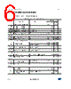
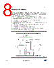
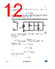
8 / 35 page  Functional description ST1S31 8/35 DocID022998 Rev 4 4 Functional description The ST1S31 device is based on a “peak current mode”, constant frequency control. The output voltage VOUT is sensed by the feedback pin (FB) compared to an internal reference (0.8 V) providing an error signal that, compared to the output of the current sense amplifier, controls the ON and OFF time of the power switch. The main internal blocks are shown in the block diagram in Figure 3. They are: A fully integrated oscillator that provides the internal clock and the ramp for the slope compensation avoiding sub-harmonic instability The soft-start circuitry to limit inrush current during the startup phase The transconductance error amplifier The pulse width modulator and the relative logic circuitry necessary to drive the internal power switches The drivers for embedded P-channel and N-channel power MOSFET switches The high-side current sensing block The low-side current sense to implement diode emulation A voltage monitor circuitry (UVLO) that checks the input and internal voltages A thermal shutdown block, to prevent thermal runaway. Figure 3. Block diagram AM11417v1 |
|
链接网址 |
| ALLDATASHEET是否为您带来帮助? [ DONATE ] |
关于 Alldatasheet | 广告服务 | 联系我们 | 隐私政策 | 数据表链接 | 链接交换 | 制造商名单 All Rights Reserved©Alldatasheet.com |
| Russian : Alldatasheetru.com | Korean : Alldatasheet.co.kr | Spanish : Alldatasheet.es | French : Alldatasheet.fr | Italian : Alldatasheetit.com Portuguese : Alldatasheetpt.com | Polish : Alldatasheet.pl | Vietnamese : Alldatasheet.vn Indian : Alldatasheet.in | Mexican : Alldatasheet.com.mx | British : Alldatasheet.co.uk | New Zealand : Alldatasheet.co.nz |
|
Family Site : ic2ic.com |
icmetro.com |
 Chinese ▼
 English
 Chinese
 German
 Japanese
 Russian
 Korean
 Spanish
 French
 Italian
 Portuguese
 Polish
 Vietnamese
 Indian
 Mexican
 British
 New Zealand