|
数据搜索系统,热门电子元器件搜索 |
|
|
数据搜索系统,热门电子元器件搜索 |
|
ST1S31D-R 数据表(PDF) 10 Page - STMicroelectronics |
|
|
|||||||||||||||||||||||||||||
ST1S31D-R 数据表(HTML) 10 Page - STMicroelectronics |
|
|
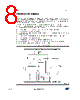
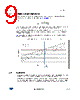
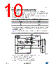
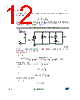
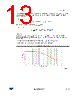
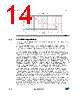
10 / 35 page  Functional description ST1S31 10/35 DocID022998 Rev 4 4.3 Error amplifier and control loop stability The error amplifier provides the error signal to be compared with the high-side switch current through the current sense circuitry. The non inverting input is connected with the internal 0.8 V reference, while the inverting input is the FB pin. The compensation network is internal and connected between the E/A output and GND. The error amplifier of the ST1S31 device is a transconductance operational amplifier, with high bandwidth and high output impedance. The ST1S31 device embeds the compensation network that assures the stability of the loop in the whole operating range. All the tools needed to check the loop stability are shown on the next pages of this section. In Figure 5 the simple small signal model for the peak current mode control loop is shown. Figure 5. Block diagram of the loop for the small signal analysis Three main terms can be identified to obtain the loop transfer function: 1. From control (output of E/A) to output, GCO(s) 2. From output (VOUT) to the FB pin, GDIV(s) 3. From the FB pin to control (output of E/A), GEA(s). The transfer function from control to output GCO(s) results: Table 5. Characteristics of the uncompensated error amplifier Description Value DC gain 94 dB gm 238 µA/V Ro 96 M L Cout Current sense Logic And Driver Slope Compensation PWM comparator Error Amp Rc Cc R1 R2 0.8V High side Switch Low side Switch GCO(s) GDIV(s) GEA(s) VIN VC VOUT VFB AM11418v1 |
|
链接网址 |
| ALLDATASHEET是否为您带来帮助? [ DONATE ] |
关于 Alldatasheet | 广告服务 | 联系我们 | 隐私政策 | 数据表链接 | 链接交换 | 制造商名单 All Rights Reserved©Alldatasheet.com |
| Russian : Alldatasheetru.com | Korean : Alldatasheet.co.kr | Spanish : Alldatasheet.es | French : Alldatasheet.fr | Italian : Alldatasheetit.com Portuguese : Alldatasheetpt.com | Polish : Alldatasheet.pl | Vietnamese : Alldatasheet.vn Indian : Alldatasheet.in | Mexican : Alldatasheet.com.mx | British : Alldatasheet.co.uk | New Zealand : Alldatasheet.co.nz |
|
Family Site : ic2ic.com |
icmetro.com |
 Chinese ▼
 English
 Chinese
 German
 Japanese
 Russian
 Korean
 Spanish
 French
 Italian
 Portuguese
 Polish
 Vietnamese
 Indian
 Mexican
 British
 New Zealand