|
数据搜索系统,热门电子元器件搜索 |
|
|
数据搜索系统,热门电子元器件搜索 |
|
ADPA7009-2ACEZ-R7 数据表(PDF) 19 Page - Analog Devices |
|
|
|||||||||||||||||||||||||||||
ADPA7009-2ACEZ-R7 数据表(HTML) 19 Page - Analog Devices |
|
|
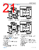
19 / 24 page  Data Sheet ADPA7009-2 APPLICATIONS INFORMATION analog.com Rev. 0 | 19 of 24 The ADPA7009-2 can be biased though VGG1 and VDD1 (north side) or VGG2 and VDD2 (south side). Figure 66 shows the primary application circuit with north-side biasing. Figure 67 shows south- side biasing. The RFIN and RFOUT pins are internally AC-coupled. Because VDD1, VDD2, VGG1, and VGG2 are internally decoupled, minimal external decoupling components are required on these pins. VGG1 and VGG2 are the gate bias pins for the amplifier. VDD1 and VDD2 are the drain bias pins for the amplifier. All measurements for this device were taken using the primary application circuit (see Figure 66). See the ADPA7009-2-EVALZ user guide for information on using the evaluation board. To avoid damaging the device, set VGG1 to −1.5 V before turning on VDD1. VGG1 can then be adjusted upwards until the desired IDQ is achieved. Then, apply the RF input signal. If the desired gate voltage is known, VGG1 can be set to that voltage value directly without taking it to the pinch off voltage (−1.5 V). To turn off the device, turn off the RF input signal, turn off VDD1, and then turn off VGG1. The VDD = 5 V and IDQ = 850 mA bias conditions are recommended to optimize overall performance. Unless otherwise noted, the data shown was taken using the recommended bias conditions. Operation of the ADPA7009-2 at different bias conditions may provide performance that differs from what is shown in Table 1 to Table 3. Biasing the ADPA7009-2 for higher drain current typically results in higher OP1dB and gain at the expense of increased power consumption (see Table 8). Data for Table 8 was taken at the following nominal bias conditions: VDD = 5 V, TCASE = 25°C, and frequency = 36 GHz. Table 8. Power Selection IDQ (mA)1 Gain (dB) OP1dB (dBm) OIP3 (dBm) PDISS (W) at PSAT 650 18.5 26.5 38.0 3.80 750 19.0 27.0 37.0 4.08 850 19.5 27.5 34.5 4.30 950 19.7 27.8 32.5 4.49 1 Adjust VGGx from −1.5 V to 0 V to achieve the desired drain current. Figure 66. Primary Application Circuit (North-Side Biasing) Figure 67. Alternate Application Circuit (South-Side Biasing) |
|
|
链接网址 |
| ALLDATASHEET是否为您带来帮助? [ DONATE ] |
关于 Alldatasheet | 广告服务 | 联系我们 | 隐私政策 | 数据表链接 | 链接交换 | 制造商名单 All Rights Reserved©Alldatasheet.com |
| Russian : Alldatasheetru.com | Korean : Alldatasheet.co.kr | Spanish : Alldatasheet.es | French : Alldatasheet.fr | Italian : Alldatasheetit.com Portuguese : Alldatasheetpt.com | Polish : Alldatasheet.pl | Vietnamese : Alldatasheet.vn Indian : Alldatasheet.in | Mexican : Alldatasheet.com.mx | British : Alldatasheet.co.uk | New Zealand : Alldatasheet.co.nz |
|
Family Site : ic2ic.com |
icmetro.com |
 Chinese ▼
 English
 Chinese
 German
 Japanese
 Russian
 Korean
 Spanish
 French
 Italian
 Portuguese
 Polish
 Vietnamese
 Indian
 Mexican
 British
 New Zealand