|
数据搜索系统,热门电子元器件搜索 |
|
|
数据搜索系统,热门电子元器件搜索 |
|
ADPA7009-2ACEZ-R7 数据表(PDF) 21 Page - Analog Devices |
|
|
|||||||||||||||||||||||||||||
ADPA7009-2ACEZ-R7 数据表(HTML) 21 Page - Analog Devices |
|
|
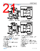
21 / 24 page  Data Sheet ADPA7009-2 BIASING THE ADPA7009-2 WITH THE HMC980LP4E analog.com Rev. 0 | 21 of 24 Figure 69. Application Circuit Using the HMC980LP4E with the ADPA7009-2 (Internal Negative Voltage Source) Figure 70. Application Circuit Using the HMC980LP4E with the ADPA7009-2 (External Negative Voltage Source) HMC980LP4E BIAS SEQUENCE The DC supply sequence described in this section is required to prevent damage to the HMC980LP4E when using the device to control the ADPA7009-2. Power-Up Sequence The power-up sequence for the HMC980LP4E is as follows: 1. Set VDIG = 3.3 V. 2. Set S0 = 3.3 V. 3. Set VDD = 5.81 V. 4. Set VNEG = −1.5 V (this step is unnecessary if using an internally generated voltage). 5. Set EN = 3.3 V (the transition from 0 V to 3.3 V turns on VGATE and VDRAIN). Power-Down Sequence The power-down sequence for the HMC980LP4E is as follows: 1. Set EN = 0 V (the transition from 3.3 V to 0 V turns off VDRAIN and VGATE). 2. Set VNEG = 0 V (this step is unnecessary if using and internally generated voltage). 3. Set VDD = 0 V. 4. Set S0 = 0 V. 5. Set VDIG = 0 V. |
|
|
链接网址 |
| ALLDATASHEET是否为您带来帮助? [ DONATE ] |
关于 Alldatasheet | 广告服务 | 联系我们 | 隐私政策 | 数据表链接 | 链接交换 | 制造商名单 All Rights Reserved©Alldatasheet.com |
| Russian : Alldatasheetru.com | Korean : Alldatasheet.co.kr | Spanish : Alldatasheet.es | French : Alldatasheet.fr | Italian : Alldatasheetit.com Portuguese : Alldatasheetpt.com | Polish : Alldatasheet.pl | Vietnamese : Alldatasheet.vn Indian : Alldatasheet.in | Mexican : Alldatasheet.com.mx | British : Alldatasheet.co.uk | New Zealand : Alldatasheet.co.nz |
|
Family Site : ic2ic.com |
icmetro.com |
 Chinese ▼
 English
 Chinese
 German
 Japanese
 Russian
 Korean
 Spanish
 French
 Italian
 Portuguese
 Polish
 Vietnamese
 Indian
 Mexican
 British
 New Zealand