|
数据搜索系统,热门电子元器件搜索 |
|
|
数据搜索系统,热门电子元器件搜索 |
|
STDRIVE102BH 数据表(PDF) 37 Page - STMicroelectronics |
|
|
|||||||||||||||||||||||||||||
STDRIVE102BH 数据表(HTML) 37 Page - STMicroelectronics |
|
|
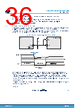
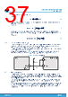
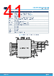
37 / 56 page  The time constant of the rising transient is: Equation 6 τEN= REN∙RPD,EN REN+RPD,EN∙CEN (6) Using the values calculated in Eq. (5) and in Eq. (6), it is possible to find the delay time required to re-arm the power MOSFETs, after a FAULT condition: Equation 7 tdelay,EN=τEN∙ln VEN,ℎigℎ−Vrelease VEN,ℎigℎ−VIH (7) According to Eq. (5), the value of REN should be chosen to be several times smaller than RPD,EN to avoid an excessive drop of the high level on the EN pin (VEN,high). In this hypothesis, it is possible to approximate Eq. (7) as: Equation 8 tdelay,EN≅REN∙CEN∙ln VDD−Vrelease VDD−VIH (8) 5.6.2 FLAG pin (STDRIVE102BH only) Unlike the UVLO protection on the VCC, the warning on the VCC supply does not disable or limit the drivers and the device functionalities. The only effect is that the FLAG pin is forced low. The external microcontroller can detect this condition and manage it by modifying the control algorithm of the driver. In case a hardwired solution is required to disable the drivers at a higher threshold than the VCC UVLO threshold, connect together the EN and the FLAG pins. A capacitor can be added as shown in Figure 27 to provide an extra delay for the enabling of the drivers: the delay is determined by the time constant τFLAG≅RFLAG∙CFLAG,explainedinthepreviousSection5.6.1. Figure 27. FLAG and EN management FLAG EN GPIO MCU STDRIVE102 VDD configuration open drain RFLAG CFLAG 5.7 Device power-up The power-up sequence starts at the rising edge of the main supply applied on the VS pin, supposing that the nSTBY pin is forced high. In case the VM and VS pins are supplied by different voltage sources, the VM voltage must be applied before the VS voltage. This sequence is not important if the nSTBY pin is kept low and it is raised after the supplies are stable. The internal 5 V regulator begins to charge the capacitor on the LGC_CAP pin. When the POR threshold is met, the internal logic starts to operate and initialize all the internal circuits. During this phase the nFAULT signal is kept low. Then, the regulators are enabled and they can charge their external bypass capacitors: most of the time required by the device to be operative is due to the charge of the external bypass capacitor. Depending on the capacitor value and the current capability of the LDO regulators and the charge pump, this time can last hundreds of microseconds. STDRIVE102BH, STDRIVE102H Device description DS14545 - Rev 1 page 37/56 |
|
链接网址 |
| ALLDATASHEET是否为您带来帮助? [ DONATE ] |
关于 Alldatasheet | 广告服务 | 联系我们 | 隐私政策 | 数据表链接 | 链接交换 | 制造商名单 All Rights Reserved©Alldatasheet.com |
| Russian : Alldatasheetru.com | Korean : Alldatasheet.co.kr | Spanish : Alldatasheet.es | French : Alldatasheet.fr | Italian : Alldatasheetit.com Portuguese : Alldatasheetpt.com | Polish : Alldatasheet.pl | Vietnamese : Alldatasheet.vn Indian : Alldatasheet.in | Mexican : Alldatasheet.com.mx | British : Alldatasheet.co.uk | New Zealand : Alldatasheet.co.nz |
|
Family Site : ic2ic.com |
icmetro.com |
 Chinese ▼
 English
 Chinese
 German
 Japanese
 Russian
 Korean
 Spanish
 French
 Italian
 Portuguese
 Polish
 Vietnamese
 Indian
 Mexican
 British
 New Zealand