|
数据搜索系统,热门电子元器件搜索 |
|
|
数据搜索系统,热门电子元器件搜索 |
|
STDRIVE102BH 数据表(PDF) 42 Page - STMicroelectronics |
|
|
|||||||||||||||||||||||||||||
STDRIVE102BH 数据表(HTML) 42 Page - STMicroelectronics |
|
|
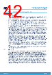
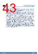
42 / 56 page  7 Layout recommendations and guidelines 7.1 Power stage layout It is very important to minimize the overall parasitic inductance of the paths connecting the power MOSFETs and the gate drivers. Higher inductance can introduce ringing on the gate signals and increase induced turn-on effects. In order to minimize inductance: • The traces between the STDRIVE102BH/H and the MOSFETs must be as short and straight as possible. • The traces should avoid multiple transitions between PCB layers. • When moving away from the STDRIVE102BH/H pads, increase the trace width (at least 0.5 mm). • Each couple of traces GHSx/OUTx and GLSx/SLSx must follow the same path and should be routed one close to the other to minimize their loop area. • Place a ground plane with no discontinuities underneath the power stage, to provide the shortest return path for the gate currents (see Section 7.2). A wide copper area must connect the drains of the three high-side MOSFETs, the motor’s supply VM and the bulk capacitors. The area can be replicated in the inner layers of the PCB; all of them can be connected using multiple vias. This approach decreases the overall impedance and improves the thermal dissipation of the high-side section of the power stage. Extend the VM copper area underneath the gate driver traces, then connect it to the VM pin of the STDRIVE102BH/H; this ensures a return path for the currents provided by the charge pump. Moreover, the VM pin is also used to sense the high-side drains for the VDS monitoring protection: wider copper areas help to reduce the voltage drop along this path. A low ESR ceramic capacitor must be placed close to the VM pin (see Section 7.3). The high-side source and the low-side drain in each half-bridge should be connected with a dedicated copper area, which then connects to each motor’s phase. Similarly, the low-side source and the shunt resistor in each half-bridge should be connected with a dedicated copper area. Each copper area can be replicated on different layers; all of them must be connected with an adequate number of vias. Vias concentration should be higher close to the pads of the power components (MOSFETs and shunt resistors). This allows to have a low impedance path for the load currents and helps to dissipate the heat. Do not use the same trace to connect different branches, even if they share the same net: for example, SLSx coming from the STDRIVE102BH/H needs a dedicated trace, which directly connects the source of the low-side MOSFET. Then a wide copper area must connect the source of the low-side MOSFET and the shunt resistor. Eventually, another dedicated pair of differential traces is routed from the two pads of the shunt resistor to the readout circuitry. Other signals not directly related to the power stage should be routed in a different area of the PCB, to avoid any noise coupling due to high dV/dt and dI/dt transients. 7.2 Grounding One inner layer of the PCB should be dedicated only for grounding. The layer should be divided in two planes: one for the power part and another for the low-voltage signal part. The two planes are tied together in correspondence with the STDRIVE102BH/H, which should be placed in the middle of the two. Power ground plane must be connected to the exposed pad (GND) of the STDRIVE102BH/H, while the signal ground plane should be connected to the AGND pin. The junction between AGND and the exposed pad (GND) must be done as close as possible to the STDRIVE102BH/H in order to minimize grounds misalignment. Exposed pad must have an adequate number of vias to transfer heat to the other layers, down to the bottom layer of the PCB, in order to dissipate heat. Therefore, the PCB can be divided in two main areas, delimited by each plane: the power area and the signal area. Routing of the components related to the operational amplifiers and in general to the circuitries related to VDD, including the resistors’ divider for TCC and IGATE pins, must be placed in the signal ground area. On the other hand, the power ground area should be dedicated only to the power stage, the gate drivers’ traces, the copper plane of the VM supply, the bulk capacitor and all the ceramic capacitors connected to each half-bridge. STDRIVE102BH, STDRIVE102H Layout recommendations and guidelines DS14545 - Rev 1 page 42/56 |
|
链接网址 |
| ALLDATASHEET是否为您带来帮助? [ DONATE ] |
关于 Alldatasheet | 广告服务 | 联系我们 | 隐私政策 | 数据表链接 | 链接交换 | 制造商名单 All Rights Reserved©Alldatasheet.com |
| Russian : Alldatasheetru.com | Korean : Alldatasheet.co.kr | Spanish : Alldatasheet.es | French : Alldatasheet.fr | Italian : Alldatasheetit.com Portuguese : Alldatasheetpt.com | Polish : Alldatasheet.pl | Vietnamese : Alldatasheet.vn Indian : Alldatasheet.in | Mexican : Alldatasheet.com.mx | British : Alldatasheet.co.uk | New Zealand : Alldatasheet.co.nz |
|
Family Site : ic2ic.com |
icmetro.com |
 Chinese ▼
 English
 Chinese
 German
 Japanese
 Russian
 Korean
 Spanish
 French
 Italian
 Portuguese
 Polish
 Vietnamese
 Indian
 Mexican
 British
 New Zealand