|
数据搜索系统,热门电子元器件搜索 |
|
|
数据搜索系统,热门电子元器件搜索 |
|
RFEVAL3-R1 数据表(PDF) 8 Page - rfsolutions.ltd |
|
|
|||||||||||||||||||||||||||||
RFEVAL3-R1 数据表(HTML) 8 Page - rfsolutions.ltd |
|
|
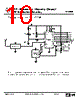
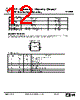
8 / 24 page  RF / IR Encoder / Decoder Chipset RF600E RF Evaluation Boards, RF600D SLEEP Holding this pin high will causes the device to run normally. Holding this pin low will causes the device to enter a sleep mode where the current drain will be 1 µA (typically). Taking the pin high will cause the device to run normally. Grounding the learn/LED pin (10) will cause the device to wake from sleep and service either a learn or erase request: on completion of the function the device will re-enter sleep mode. Note that while in sleep mode the S0 – S4 and low battery outputs will held high. Notes to obtain Minimal Current consumption Sleep/run applications will require close attention to external circuitry in order to minimise the sleep current and allow a typical circuit draw of 1 µA at +5 volts (with/without optional external eeprom). With reference to the application schematic, the following should be noted; 1. Fit an additional 2.2M Ω resistor from pin 10 to +5 volts. 2. Fit an additional 2.2M Ω resistor from pin 3 to +5 volts. 3. Connect controlling drive to pin 13: high for run and low for sleep. 4. The S0 – S4 and low battery outputs are not asserted during sleep and will have to be sampled by the controlling micro controller during run mode. 5. The S0 – S4 and low battery LED’s are not required as part of the circuit and can be omitted of required. 6. Incoming data mark selection on pin 7 MUST be by a resistor (typically 22K) to either +5 or ground and NOT by a direct connection. 7. The RF/IR data input (pin 9) must be at a valid logic level at all times. In sleep mode, if this input is allowed to float then significant device current may flow. DS600-9 Sept ‘04 ©2004 Reg. No. 227 4001, ENGLAND Page 8 |
|
|
链接网址 |
| ALLDATASHEET是否为您带来帮助? [ DONATE ] |
关于 Alldatasheet | 广告服务 | 联系我们 | 隐私政策 | 数据表链接 | 链接交换 | 制造商名单 All Rights Reserved©Alldatasheet.com |
| Russian : Alldatasheetru.com | Korean : Alldatasheet.co.kr | Spanish : Alldatasheet.es | French : Alldatasheet.fr | Italian : Alldatasheetit.com Portuguese : Alldatasheetpt.com | Polish : Alldatasheet.pl | Vietnamese : Alldatasheet.vn Indian : Alldatasheet.in | Mexican : Alldatasheet.com.mx | British : Alldatasheet.co.uk | New Zealand : Alldatasheet.co.nz |
|
Family Site : ic2ic.com |
icmetro.com |
 Chinese ▼
 English
 Chinese
 German
 Japanese
 Russian
 Korean
 Spanish
 French
 Italian
 Portuguese
 Polish
 Vietnamese
 Indian
 Mexican
 British
 New Zealand