|
数据搜索系统,热门电子元器件搜索 |
|
|
数据搜索系统,热门电子元器件搜索 |
|
ADP2441ACPZ-R2 数据表(PDF) 18 Page - Analog Devices |
|
|
|||||||||||||||||||||||||||||
ADP2441ACPZ-R2 数据表(HTML) 18 Page - Analog Devices |
|
|
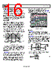
18 / 32 page  ADP2441 Data Sheet Rev. A | Page 18 of 32 APPLICATIONS INFORMATION SELECTING THE OUTPUT VOLTAGE The output voltage is set using a resistor divider connected between the output voltage and the FB pin (see Figure 54). The resistor divider divides down the output voltage to the 0.6 V FB regulation voltage. The output voltage can be set to as low as 0.6 V and as high as 90% of the power input voltage. The ratio of the resistive voltage divider sets the output voltage, and the absolute value of the resistors sets the divider string current. For lower divider string currents, the small 50 nA (0.1 μA maximum) FB bias current should be taken into account when calculating the resistor values. The FB bias current can be ignored for a higher divider string current; however, using small feedback resistors degrades efficiency at very light loads. To limit degradation of the output voltage accuracy due to FB bias current to less than 0.005% (0.5% maximum), ensure that the divider string current is greater than 20 μA. To calculate the desired resistor values, first determine the value of the bottom resistor, RBOTTOM, as follows: STRING REF BOTTOM I V R (2) where: VREF is the internal reference and equals 0.6 V. ISTRING is the resistor divider string current. Then calculate the value of the top resistor, RTOP, as follows: REF REF OUT BOTTOM TOP V V V R R (3) ADP2441 FB RTOP RFREQ CSS VOUT RBOTTOM PGOOD EXTERNAL SUPPLY FREQ SS/TRK Figure 54. Voltage Divider Table 5. Output Voltage Selection Voltage (V) RTOP (kΩ) RBOTTOM (kΩ) 12 190 10 5 73 10 3.3 45 10 1.2 10 10 SETTING THE SWITCHING FREQUENCY The choice of the switching frequency depends on the required dc-to-dc conversion ratio and is limited by the minimum and maximum controllable duty cycle, as shown in Figure 55. This is due to the requirement of minimum on time and minimum off time for current sensing and robust operation. However, the choice is also influenced by whether there is a need for small external components. For example, for small, area limited power solutions, higher switching frequencies are required. 0 10 20 30 40 50 60 70 80 90 100 0 200 400 600 800 1000 1200 FREQUENCY (kHz) DMAX DMIN Figure 55. Duty Cycle vs. Switching Frequency Calculate the value of the frequency resistor using the following equation: SW FREQ f R 500 , 92 (4) where RFREQ is in kΩ, and fSW is in kHz. Table 6 and Figure 56 provide examples of frequency resistor values, which are based on the switching frequency. Table 6. Frequency Resistor Selection RFREQ (kΩ) Frequency 308 300 kHz 132 700 kHz 92.5 1 MHz 200 300 400 500 600 700 800 900 1000 1100 1200 50 100 150 200 250 300 350 RESISTANCE (kΩ) Figure 56. Frequency vs. Resistance |
|
链接网址 |
| ALLDATASHEET是否为您带来帮助? [ DONATE ] |
关于 Alldatasheet | 广告服务 | 联系我们 | 隐私政策 | 数据表链接 | 链接交换 | 制造商名单 All Rights Reserved©Alldatasheet.com |
| Russian : Alldatasheetru.com | Korean : Alldatasheet.co.kr | Spanish : Alldatasheet.es | French : Alldatasheet.fr | Italian : Alldatasheetit.com Portuguese : Alldatasheetpt.com | Polish : Alldatasheet.pl | Vietnamese : Alldatasheet.vn Indian : Alldatasheet.in | Mexican : Alldatasheet.com.mx | British : Alldatasheet.co.uk | New Zealand : Alldatasheet.co.nz |
|
Family Site : ic2ic.com |
icmetro.com |
 Chinese ▼
 English
 Chinese
 German
 Japanese
 Russian
 Korean
 Spanish
 French
 Italian
 Portuguese
 Polish
 Vietnamese
 Indian
 Mexican
 British
 New Zealand