|
数据搜索系统,热门电子元器件搜索 |
|
|
数据搜索系统,热门电子元器件搜索 |
|
ADP2441ACPZ-R2 数据表(PDF) 19 Page - Analog Devices |
|
|
|||||||||||||||||||||||||||||
ADP2441ACPZ-R2 数据表(HTML) 19 Page - Analog Devices |
|
|
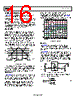
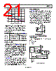
19 / 32 page  Data Sheet ADP2441 Rev. A | Page 19 of 32 SOFT START The soft start function limits the input inrush current and prevents output overshoot at startup. The soft start time is programmed by connecting a small ceramic capacitor between the SS/TRK and AGND pins, with the value of this capacitor defining the soft start time, tSS, as follows: SS SS SS REF C I t V (5) where: VREF is the internal reference voltage and equals 0.6 V. ISS is the soft start current and equals 1 μA. CSS is the soft start capacitor value. Table 7. Soft Start Time Selection Soft Start Capacitor (nF) Soft Start Time (ms) 5 3 10 6 20 12 Alternatively, the user can float the SS/TRK pin and use the internal soft start time of 2 ms. EXTERNAL COMPONENTS SELECTION Input Capacitor Selection The input current to a buck regulator is pulsating in nature. The current is zero when the high-side switch is off and is approxi- mately equal to the load current when the switch is on. Because switching occurs at reasonably high frequencies (300 kHz to 1 MHz), the input bypass capacitor usually supplies most of the high frequency current (ripple current), allowing the input power source to supply only the average (dc) current. The input capacitor needs a sufficient ripple current rating to handle the input ripple and needs an ESR that is low enough to mitigate the input voltage ripple. In many cases, different types of capacitors are placed in parallel to minimize the effective ESR and ESL. The minimum input capacitance required for a particular load is SW ESR OUT PP OUT MIN IN f R D I V D D I C ) ( ) 1 ( _ (6) where: VPP is the desired input ripple voltage. RESR is the equivalent series resistance of the capacitor. IOUT is the maximum load current. It is recommended to use a ceramic bypass capacitor because the ESR associated with this type of capacitor is near zero, simplifying the equation to SW PP OUT MIN IN f V D D I C ) 1 ( _ (7) In addition, it is recommended to use a ceramic capacitor with a voltage rating that is 1.5 times the input voltage with X5R and X7R dielectrics. Using Y5V and Z5U dielectrics is not recommended due to their poor temperature and dc bias characteristics. Table 10 shows a list of recommended MLCC capacitors from Murata and Taiyo Yuden. For large step load transients, add more bulk capacitance by, for example, using electrolytic or polymer capacitors. Make sure that the ripple current rating of the bulk capacitor exceeds the minimum input ripple current of a particular design. Inductor Selection The high switching frequency of the ADP2441 allows for minimal output voltage ripple even when small inductors are used. Selecting the size of the inductor involves considering the trade-off between efficiency and transient response. A smaller inductor results in larger inductor current ripple, which provides excellent transient response but degrades efficiency. Due to the high switching frequency of the ADP2441, using shielded ferrite core inductors is recommended because of their low core losses and low EMI. The inductor ripple current also affects the stability of the loop because the ADP2441 uses the emulated peak current mode architecture. In the traditional approach of slope compensation, the user sets the inductor ripple current and then sets the slope compensation using an external ramp resistor. In most cases, the inductor ripple current is typically set to be 1/3 of the maximum load current for optimal transient response and efficiency. The ADP2441 has internal slope compensation, which assumes that the inductor ripple current is set to 0.3 A (30% of the maximum load of 1 A), eliminating the need for an external ramp resistor. For the ADP2441, choose an inductor such that the peak-to- peak ripple current of the inductor is between 0.2 A and 0.5 A for stable operation. Therefore, calculate the inductor value as follows: L f V V V V I SW IN OUT IN OUT L ) ( (8) 0.2 A ≤ ΔIL ≤ 0.5 A SW IN OUT IN OUT SW IN OUT IN OUT f V V V V L f V V V V ) ( 5 ) ( 2 SW IN OUT IN OUT IDEAL f V V V V L ) ( 3 . 3 (9) where: VIN is the input voltage. VOUT is the desired output voltage. fSW is the regulator switching frequency. For applications with a wide input (VIN) range, choose the inductor based on the geometric mean of the input voltage extremes. MIN IN MAX IN GEOMETRIC IN V V V _ _ ) ( where: VIN_MAX is the maximum input voltage. VIN_MIN is the minimum input voltage. |
|
链接网址 |
| ALLDATASHEET是否为您带来帮助? [ DONATE ] |
关于 Alldatasheet | 广告服务 | 联系我们 | 隐私政策 | 数据表链接 | 链接交换 | 制造商名单 All Rights Reserved©Alldatasheet.com |
| Russian : Alldatasheetru.com | Korean : Alldatasheet.co.kr | Spanish : Alldatasheet.es | French : Alldatasheet.fr | Italian : Alldatasheetit.com Portuguese : Alldatasheetpt.com | Polish : Alldatasheet.pl | Vietnamese : Alldatasheet.vn Indian : Alldatasheet.in | Mexican : Alldatasheet.com.mx | British : Alldatasheet.co.uk | New Zealand : Alldatasheet.co.nz |
|
Family Site : ic2ic.com |
icmetro.com |
 Chinese ▼
 English
 Chinese
 German
 Japanese
 Russian
 Korean
 Spanish
 French
 Italian
 Portuguese
 Polish
 Vietnamese
 Indian
 Mexican
 British
 New Zealand