|
数据搜索系统,热门电子元器件搜索 |
|
|
数据搜索系统,热门电子元器件搜索 |
|
YMF754-R 数据表(PDF) 18 Page - YAMAHA CORPORATION |
|
|
|||||||||||||||||||||||||||||
YMF754-R 数据表(HTML) 18 Page - YAMAHA CORPORATION |
|
|
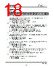
18 / 60 page  YMF754 June 28, 1999 -18- 40-41h: Legacy Audio Control Read / Write Default: 907Fh Access Bus Width: 8, 16, 32-bit b15 b14 b13 b12 b11 b10 b9 b8 b7 b6 b5 b4 b3 b2 b1 b0 LAD SIEN MPUIRQ SBIRQ SDMA I/O MIEN MEN JPEN FMEN SBEN b0................SBEN: Sound Blaster Enable This bit enables the mapping of the Sound Blaster Pro block in the I/O space specified by 62-63h: Sound Blaster Base Address register, when LAD is set to “0”. “0”: Disable the mapping of the SB block to the I/O space “1”: Enable the mapping of the SB block to the I/O space (default) b1................FMEN: FM Synthesizer Enable This bit enables the mapping of the FM Synthesizer block in the I/O space specified by 60-61h: FM Synthesizer Base Address register when LAD is set to “0”. FM Synthesizer registers can be accessed via SB I/O space, while the SB block is enabled, even if FMEN is set to “0”. “0”: Disable the mapping of the FM Synthesizer block to the FMIO space “1”: Enable the mapping of the FM Synthesizer block to the FMIO space (default) After setting FMEN to “1”, about 100 msec is necessary before accessing these I/O space. b2................JPEN: Joystick Port Enable This bit enables the mapping of the Joystick block in the I/O space specified by 66-67h: Joystick Base Address register, when LAD is set to “0”. “0”: Disable the mapping of the Joystick block “1”: Enable the mapping of the Joystick block (default) b3................MEN: MPU401 Enable This bit enables the mapping of the MPU401 block in the I/O space specified by 64-65h: MPU401 Base Address register, when LAD is set to “0”. “0”: Disable the mapping of the MPU401 block “1”: Enable the mapping of the MPU401 block (default) b4................MIEN: MPU401 IRQ Enable This bit enables the interrupt service of MPU401, when LAD is set to “0” and MEN is set to “1”. MPU401 generates an interrupt signal when it receives any kind of MIDI data from the RXD pin. “0”: The MPU401 block can not use the interrupt service. “1”: The MPU401 block can use interrupt signals determined by the MPUIRQ bits. (default) b5................I/O: I/O Address Aliasing Control This bit selects the number of bits to decode for the I/O address of each block. “0”: 16-bit address decode “1”: 10-bit address decode (default) |
|
链接网址 |
| ALLDATASHEET是否为您带来帮助? [ DONATE ] |
关于 Alldatasheet | 广告服务 | 联系我们 | 隐私政策 | 数据表链接 | 链接交换 | 制造商名单 All Rights Reserved©Alldatasheet.com |
| Russian : Alldatasheetru.com | Korean : Alldatasheet.co.kr | Spanish : Alldatasheet.es | French : Alldatasheet.fr | Italian : Alldatasheetit.com Portuguese : Alldatasheetpt.com | Polish : Alldatasheet.pl | Vietnamese : Alldatasheet.vn Indian : Alldatasheet.in | Mexican : Alldatasheet.com.mx | British : Alldatasheet.co.uk | New Zealand : Alldatasheet.co.nz |
|
Family Site : ic2ic.com |
icmetro.com |
 Chinese ▼
 English
 Chinese
 German
 Japanese
 Russian
 Korean
 Spanish
 French
 Italian
 Portuguese
 Polish
 Vietnamese
 Indian
 Mexican
 British
 New Zealand