|
数据搜索系统,热门电子元器件搜索 |
|
|
数据搜索系统,热门电子元器件搜索 |
|
LMX2430 数据表(PDF) 34 Page - National Semiconductor (TI) |
|
|
|
|||||||||||||||||||||||||||||
LMX2430 数据表(HTML) 34 Page - National Semiconductor (TI) |
|
|
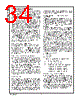
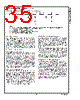
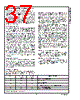
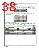
34 / 49 page  1.0 Functional Description The basic phase-lock-loop (PLL) configuration consists of a high-stability crystal reference oscillator, a frequency synthe- sizer such as the National Semiconductor LMX243x, a volt- age controlled oscillator (VCO), and a passive loop filter. The frequency synthesizer includes a phase detector, current mode charge pump, programmable reference R and feed- back N frequency dividers. The VCO frequency is estab- lished by dividing the crystal reference signal down via the reference divider to obtain a comparison reference fre- quency. This reference signal, f r, is then presented to the input of a phase/ frequency detector and compared with the feedback signal, f p, which was obtained by dividing the VCO frequency down by way of the feedback divider. The phase/ frequency detector measures the phase error between the f r and f p signals and outputs control signals that are directly proportional to the phase error. The charge pump then pumps charge into or out of the loop filter based on the magnitude and direction of the phase error. The loop filter converts the charge into a stable control voltage for the VCO. The phase/frequency detector’s function is to adjust the voltage presented to the VCO until the feedback signal’s frequency and phase match that of the reference signal. When this “Phase-Locked” condition exists, the VCO fre- quency will be N times that of the comparison frequency, where N is the feedback divider ratio. 1.1 REFERENCE OSCILLATOR INPUT The reference oscillator frequency for both the RF and IF PLLs is provided from an external reference via the OSCin pin. The reference buffer circuit supports input frequencies from 5 to 40 MHz with a minimum input sensitivity of 0.5 V PP. The reference buffer circuit has an approximate Vcc/2 input threshold and can be driven from an external AC coupled source. Typically, the OSCin pin is connected to the output of a crystal oscillator. 1.2 REFERENCE DIVIDERS (R COUNTERS) The reference dividers divide the reference input signal, OSCin, by a factor of R. The output of the reference divider circuits feeds the reference input of the phase detector. This reference input to the phase detector is often referred to as the comparison frequency. The divide ratio should be chosen such that the maximum phase comparison frequency (f COM- PRF or f COMPIF) of 10 MHz is not exceeded. The RF and IF reference dividers are each comprised of 15-bit CMOS binary counters that support a continuous in- teger divide ratio from 3 to 32767. The RF and IF reference divider circuits are clocked by the output of the reference buffer circuit which is common to both. Refer to Sections 2.4.1 and 2.7.1 for details on how to program the RF_R and IF_R counters. 1.3 PRESCALERS The FinRF and FinIF input pins drive the input of a differential-pair amplifier. The output of the differential-pair amplifier drives a chain of D-type flip-flops in a dual modulus configuration. The output of the prescaler is used to clock the subsequent feedback dividers. The RF PLL complementary inputs can be driven differentially, or the negative input can be AC coupled to ground through an external capacitor for single ended configuration. A 16/17 or a 32/33 prescale ratio can be selected for the 5.0 GHz LMX2434 RF synthesizer. An 8/9 or a 16/17 prescale ratio can be selected for both the LMX2430 and LMX2433 RF synthesizers. The IF PLL is single ended. An 8/9 or a 16/17 prescale ratio can be se- lected for the IF synthesizer. 1.4 PROGRAMMABLE FEEDBACK DIVIDERS (N COUNTERS) The programmable feedback dividers operate in concert with the prescalers to divide the input signal, Fin, by a factor of N. The output of the programmable reference divider is pro- vided to the feedback input of the phase detector circuit. The divide ratio should be chosen such that the maximum phase comparison frequency (f COMPRF or fCOMPIF) of 10 MHz is not exceeded. The programmable feedback divider circuit is comprised of an A counter (swallow counter) and a B counter (program- mble binary counter). For both the LMX2430 and LMX2433, the RF_A counter is a 4-bit swallow counter, programmable from 0 to 15. The LMX2434 RF_A counter is a 5-bit swallow counter, programmable from 0 to 31. The LMX243x IF_A counter is a 4-bit swallow counter, programmable from 0 to 15. For both the LMX2430 and LMX2433, the RF_B counter is a 15-bit binary counter, programmable from 3 to 32767. The LMX2434 RF_B counter is a 14-bit binary counter, programmable from 3 to 16383. The LMX243x IF_B is a 14-bit binary counter programmable from 3 to 16383. A continuous integer divide ratio is achieved if N ≥ P * (P−1), where P is the value of the prescaler selected. Divide ratios less than the minimum continuous divide ratio are achiev- able as long as the binary programmable counter value is greater than the swallow counter value (B ≥ A). Refer to Sections 2.5.1.1, 2.5.1.2, 2.5.2.1, 2.5.2.2, 2.8.1, and 2.8.2 for details on how to program the A and B counters. The following equations are useful in determining and program- ming a particular value of N: N=(P x B) + A Fin = Nxf COMP Definitions: f COMP: RF or IF phase detector comparison frequency Fin: RF or IF input frequency A: RF_A or IF_A counter value B: RF_B or IF_B counter value P: Preset modulus of the dual moduIus prescaler LMX2430 RF synthesizer: P = 8 or 16 LMX2433 RF synthesizer: P = 8 or 16 LMX2434 RF synthesizer: P = 16 or 32 LMX243x IF synthesizer: P = 8 or 16 1.5 PHASE/ FREQUENCY DETECTORS The RF and IF phase/ frequency detectors (PFD) are driven from their respective N and R counter outputs. The maxi- mum frequency for both the RF and IF phase detector inputs is 10 MHz. The PFD outputs control the respective charge pumps. The polarity of the pump-up or pump-down control signals are programmed using the RF_CPP or IF_CPP con- trol bits, depending on whether the RF or IF VCO character- istics are positive or negative. Refer to Sections 2.4.2 and 2.7.2 for more details. The PFDs have a detection range of −2 π to +2π. The PFDs also receive a feedback signal from the charge pump in order to eliminate dead zone. www.national.com 34 |
|
链接网址 |
| ALLDATASHEET是否为您带来帮助? [ DONATE ] |
关于 Alldatasheet | 广告服务 | 联系我们 | 隐私政策 | 数据表链接 | 链接交换 | 制造商名单 All Rights Reserved©Alldatasheet.com |
| Russian : Alldatasheetru.com | Korean : Alldatasheet.co.kr | Spanish : Alldatasheet.es | French : Alldatasheet.fr | Italian : Alldatasheetit.com Portuguese : Alldatasheetpt.com | Polish : Alldatasheet.pl | Vietnamese : Alldatasheet.vn Indian : Alldatasheet.in | Mexican : Alldatasheet.com.mx | British : Alldatasheet.co.uk | New Zealand : Alldatasheet.co.nz |
|
Family Site : ic2ic.com |
icmetro.com |
 Chinese ▼
 English
 Chinese
 German
 Japanese
 Russian
 Korean
 Spanish
 French
 Italian
 Portuguese
 Polish
 Vietnamese
 Indian
 Mexican
 British
 New Zealand