|
数据搜索系统,热门电子元器件搜索 |
|
|
数据搜索系统,热门电子元器件搜索 |
|
LMX2430 数据表(PDF) 35 Page - National Semiconductor (TI) |
|
|
|
|||||||||||||||||||||||||||||
LMX2430 数据表(HTML) 35 Page - National Semiconductor (TI) |
|
|
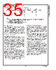
35 / 49 page  1.0 Functional Description (Continued) 1.5.1 Phase Comparator and Internal Charge Pump Characteristics 20053511 Notes: 1. The minimum width of the pump-up and pump-down current pulses occur at the CPoutRF or CPoutIF pins when the loop is phase locked. 2. The diagram assumes positive VCO characteristics, i.e. RF_CPP or IF_CPP = 1. 3. fr is the PFD input from the reference divider (R counter). 4. fp is the PFD input from the programmable feedback divder (N counter). 5. CPout refers to either the RF or IF charge pump output. 1.6 CHARGE PUMPS The charge pump directs charge into or out of an external loop filter. The loop filter converts the charge into a stable control voltage which is applied to the tuning input of the VCO. The charge pump steers the VCO control voltage towards Vcc during pump-up events and towards GND dur- ing pump-down events. When locked, CPoutRF or CPoutIF are primarily in a TRI-STATE mode with small corrections occuring at the phase comparator rate. The charge pump output current magnitude can be selected by toggling the RF_CPG or IF_CPG control bits. 1.7 MICROWIRE SERIAL INTERFACE The programmable register set is accessed via the MI- CROWIRE serial interface. A low voltage logic interface allows direct connection to 1.8V devices. The interface is comprised of three signal pins: CLK, DATA and LE. Serial data is clocked into the 24-bit shift register on the rising edge of CLK. The last two bits decode the internal control register address. When LE transitions HIGH, DATA stored in the shift register is loaded into one of four control registers depending on the state of the address bits. The MSB of DATA is loaded in first. The synthesizers can be programmed even in power down mode. A complete programming description is pro- vided in Section 2.0 Programming Description. 1.8 MULTI-FUNCTION OUTPUTS The LMX243x device’s Ftest/LD output pin is a multi-function output that can be configured as a general purpose CMOS TRI-STATE output, push-pull analog lock detect output, open-drain analog lock detect output, digital filtered lock detect output, or used to monitor the output of the various reference divider (R counter) or feedback divider (N counter) circuits. The Ftest/LD control word is used to select the desired output function. When the PLL is in powerdown mode, the Ftest/LD output is disabled and is in a high impedance state. A complete programming description of the multi-function output is provided in Section 2.10. 1.8.1 Push-Pull Analog Lock Detect Output An analog lock detect status generated from the phase detector is available on the Ftest/LD output pin if selected. A push-pull configuration can be selected for the lock detect output signal. With this configuration, the lock detect output goes HIGH when the charge pump is inactive. It goes LOW when the charge pump is active during a comparison cycle. Narrow low going pulses are observed when the charge pump turns on. There are three separate push-pull analog lock detect sig- nals that are routed to the multiplexer. Two of these monitor the lock status of the individual synthesizers. The third de- tects the condition when both the RF and IF synthesizers are in a locked state. External circuitry is required to provide a steady DC signal to indicate when the PLL is in a locked state. Refer to Section 2.10 for details on how to program the different push-pull analog lock detect options. 1.8.2 Open-Drain Analog Lock Detect Output The lock detect output can be an open-drain configuration. In this configuration, the lock detect output goes to a high impedance state when the charge pump is inactive. It goes LOW when the charge pump is active during a comparison cycle. When a pull-up resistor is used, narrow low going pulses are observed when the charge pump turns on. Similarly, three separate open-drain analog lock detect sig- nals are routed to the multiplexer. Two of these monitor the lock status of the individual synthesizers. The third detects the condition when both the RF and IF synthesizers are in a locked state. External circuitry is required to provide a steady DC signal to indicate when the PLL is in a locked state. Refer to Section 2.10 for details on how to program the different open-drain analog lock detect options. www.national.com 35 |
|
链接网址 |
| ALLDATASHEET是否为您带来帮助? [ DONATE ] |
关于 Alldatasheet | 广告服务 | 联系我们 | 隐私政策 | 数据表链接 | 链接交换 | 制造商名单 All Rights Reserved©Alldatasheet.com |
| Russian : Alldatasheetru.com | Korean : Alldatasheet.co.kr | Spanish : Alldatasheet.es | French : Alldatasheet.fr | Italian : Alldatasheetit.com Portuguese : Alldatasheetpt.com | Polish : Alldatasheet.pl | Vietnamese : Alldatasheet.vn Indian : Alldatasheet.in | Mexican : Alldatasheet.com.mx | British : Alldatasheet.co.uk | New Zealand : Alldatasheet.co.nz |
|
Family Site : ic2ic.com |
icmetro.com |
 Chinese ▼
 English
 Chinese
 German
 Japanese
 Russian
 Korean
 Spanish
 French
 Italian
 Portuguese
 Polish
 Vietnamese
 Indian
 Mexican
 British
 New Zealand