|
数据搜索系统,热门电子元器件搜索 |
|
|
数据搜索系统,热门电子元器件搜索 |
|
LMX2430 数据表(PDF) 37 Page - National Semiconductor (TI) |
|
|
|
|||||||||||||||||||||||||||||
LMX2430 数据表(HTML) 37 Page - National Semiconductor (TI) |
|
|
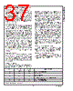
37 / 49 page  1.0 Functional Description (Continued) 1.8.4 Reference Divider and Feedback Divider Output The outputs of the various N and R dividers can be moni- tored by selecting the appropriate Ftest/LD word. This is essential when performing OSCin or Fin sensitivity measure- ments. Refer to the LMX243x FinRF Sensitivity Test Setup or LMX243x OSCin Sensitivity Test Setup sections for more details. Note, the R and N outputs that are routed to the Ftest/LD are R/2 and N/2 respectively. The internal /2 circuit is used to provide a 50% duty cycle. Refer to Section 2.10 for more details on how to route the appropriate divider output to the Ftest/LD pin. 1.9 FASTLOCK OUTPUT The LMX243x Fastlock feature allows a faster loop response time during lock aquisition. The loop response time (lock time) can be approximately halved if the loop bandwidth is doubled. In order to achieve this, the same gain/ phase relationship should be maintained when the loop bandwidth is doubled. When the FLoutRF or OSCout/ FLoutIF pins are configured as FastLock outputs, an open drain device is enabled. The open drain device switches in a resistor paral- lel, and of equal value, to R2 of the external loop filter. The loop bandwidth is effectively doubled and stability is main- tained. Once locked to the correct frequency, the PLL will return to a steady state condition.The LMX243x offers two methods to achieve Fastlock: manual and automatic. Manual Fastlock is achieved by increasing the charge pump current from 1 mA (RF_CPG/ IF_CPG Bit = 0) in the steady state mode, to 4 mA (RF_CPG/ IF_CPG Bit = 1) in Fastlock mode. Automatic Fastlock is achieved by programming the timeout counter register (RF_TOC/ IF_TOC) with the appro- priate number of phase comparison cycles that the RF/ IF synthesizer will spend in the Fastlock state. Refer to Sec- tions 2.6 and 2.9 for details on how to configure the FLoutRF or OSCout/ FLoutIF output to an open drain Fast- lock output. 1.10 COUNTER RESET When the RF_RST/ IF_RST bit is enabled, both the feed- back divider (RF_N/ IF_N) and reference divider (RF_R/ IF_R) are held at their load point. When the device is pro- grammed to normal operation, both the feedback divider and reference divder are enabled and resume counting in close alignment to each other. Refer to Sections 2.4.5 and 2.7.5 for more details. 1.11 POWER CONTROL The LMX243x device can be asynchronously powered down when the EN pin is set LOW, independent of the state of the powerdown bits. Note that the OSCout/ FLoutIF pin can still be enabled if the ENosc pin is set HIGH, independent of the state of the EN pin. This capability allows the oscillator buffer to be used as a crystal oscillator. When EN is set HIGH, powerdown is controlled through the MICROWIRE. The powerdown word is comprised of the RF_PD/ IF_PD bit, in conjuction with the RF_CPT/ IF_CPT bit. The powerdown control word is used to set the operating mode of the device. Refer to Sections 2.4.4, 2.5.4, 2.7.4, and 2.8.4 for details on how to program the RF or IF powerdown bits. When either synthesizer is powered down, the respective prescaler, phase detector, and charge pump circuit is dis- abled. The CPoutRF/ CPoutIF, FinRF/ FinIF, and FinRF* pins are all forced to a high impedance state. The reference divider and feedback divider circuits are held at the load point during powerdown. The oscillator buffer is disabled when the ENosc pin is set LOW. The OSCin pin is forced to a HIGH state through an approximate 100 k Ω resistance when this condition exists. When either synthesizer is acti- vated, the respective prescaler, phase detector, charge pump circuit, and the oscillator buffer are all powered up. The feedback divider and reference divider are held at their load point. This allows the reference oscillator, feedback divider, reference divider and prescaler circuitry to reach proper bias levels. After a finite delay, the feedback and reference dividers are enabled and they resume counting in close alignment (the maximum error is one prescaler cycle). The MICROWIRE control register remains active and ca- pable of loading and latching data while in powerdown mode. 1.11.1 Synchronous Powerdown Mode In this mode, the powerdown function is gated by the charge pump. When the device is configured for synchronous pow- erdown, the device will enter the powerdown mode upon completion of the next charge pump pulse event. 1.11.2 Asynchronous Powerdown Mode In this mode, the powerdown function is NOT gated by the completion of a charge pump pulse event. When the device is configured for asynchronous powerdown, the part will go into powerdown mode immediately. EN Pin RF_CPT/ IF_CPT Bit RF_PD/ IF_PD Bit Operating Mode 0 X X Asynchronous Powerdown 1 0 0 PLL Active. Normal Operation 1 1 0 PLL Active. Charge Pump Output in High Impedance State 1 0 1 Synchronous Powerdown 1 1 1 Asynchronous Powerdown Note: X refers to a don’t care condition. www.national.com 37 |
|
链接网址 |
| ALLDATASHEET是否为您带来帮助? [ DONATE ] |
关于 Alldatasheet | 广告服务 | 联系我们 | 隐私政策 | 数据表链接 | 链接交换 | 制造商名单 All Rights Reserved©Alldatasheet.com |
| Russian : Alldatasheetru.com | Korean : Alldatasheet.co.kr | Spanish : Alldatasheet.es | French : Alldatasheet.fr | Italian : Alldatasheetit.com Portuguese : Alldatasheetpt.com | Polish : Alldatasheet.pl | Vietnamese : Alldatasheet.vn Indian : Alldatasheet.in | Mexican : Alldatasheet.com.mx | British : Alldatasheet.co.uk | New Zealand : Alldatasheet.co.nz |
|
Family Site : ic2ic.com |
icmetro.com |
 Chinese ▼
 English
 Chinese
 German
 Japanese
 Russian
 Korean
 Spanish
 French
 Italian
 Portuguese
 Polish
 Vietnamese
 Indian
 Mexican
 British
 New Zealand