|
数据搜索系统,热门电子元器件搜索 |
|
|
数据搜索系统,热门电子元器件搜索 |
|
AD8067ART-R2 数据表(PDF) 15 Page - Analog Devices |
|
|
|||||||||||||||||||||||||||||
AD8067ART-R2 数据表(HTML) 15 Page - Analog Devices |
|
|
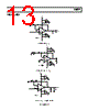
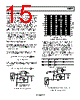
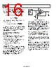
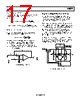
15 / 24 page  AD8067 Rev. 0 | Page 15 of 24 THEORY OF OPERATION FREQUENCY – MHz 90 0 10 20 30 40 50 60 70 80 –10 120 –150 –120 –90 –60 –30 0 30 60 90 –180 0.01 0.1 1 10 100 1k PHASE GAIN The AD8067 is a low noise, wideband, voltage feedback operational amplifier that combines a precision JFET input stage with Analog Devices’ dielectrically isolated eXtra Fast Complementary Bipolar (XFCB) process BJTs. Operating supply voltages range from 5 V to 24 V. The amplifier features a patented rail-to-rail output stage capable of driving within 0.25 V of either power supply while sourcing or sinking 30 mA. The JFET input, composed of N-channel devices, has a common-mode input range that includes the negative supply rail and extends to 3 V below the positive supply. In addition, the potential for phase reversal behavior has been eliminated for all input voltages within the power supplies. The combination of low noise, dc precision, and high bandwidth makes the AD8067 uniquely suited for wideband, very high input impedance, high gain buffer applications. It will also prove useful in wideband transimpedance applications, such as a photodiode interface, that require very low input currents and dc precision. Figure 41. Open-Loop Frequency Response Basic Frequency Response The bandwidth formula only holds true when the phase margin of the application approaches 90°, which it will in high gain config- urations. The bandwidth of the AD8067 used in a G = +10 buffer is 54 MHz, considerably faster than the 30 MHz predicted by the closed loop –3 dB frequency equation. This extended bandwidth is due to the phase margin being at 60° instead of 90°. Gains lower than +10 will show an increased amount of peaking, as shown in Figure 4. For gains lower than +7, use the AD8065, a unity gain stable JFET input op amp with a unity gain bandwidth of 145 MHz, or refer to the Applications section for using the AD8067 in a gain of 2 configuration. The AD8067’s typical open-loop response (see Figure 41) shows a phase margin of 60° at a gain of +10. Typical configurations for noninverting and inverting voltage gain applications are shown in Figure 40 and Figure 42. The closed-loop frequency response of a basic noninverting gain configuration can be approximated using the equation: () () G F G R R R GBP Frequency dB – Loop Closed + × = 3 Gain RG (Ω) RF (kΩ) BW (MHz) 10 110 1 54 20 49.9 1 15 50 20 1 6 100 10 1 3 1 + = G F /R R Gain DC GBP is the gain bandwidth product of the amplifier. Typical GBP for the AD8067 is 300 MHz. See Table 1 for recommended values of RG and RF. Table 1. Recommended Values of RG and RF 1 R R Gain Noise ion Configurat ng Noninverti G F + = +VS AD8067 + – RX RLOAD + VOUT – RF 10 µF 0.1 µF 10 µF 0.1 µF –VS RG RS SIGNAL SOURCE VI FOR BEST PERFORMANCE, SET RX = (RS + RG) || RF + + +VS AD8067 + – RX RLOAD + VOUT – RF FOR BEST PERFORMANCE, SET RS + RX = RG || RF 10 µF 0.1 µF 10 µF + 0.1 µF RG RS SIGNAL SOURCE –VS VI + Figure 40. Noninverting Gain Configuration Figure 42. Inverting Gain Configuration |
|
|
链接网址 |
| ALLDATASHEET是否为您带来帮助? [ DONATE ] |
关于 Alldatasheet | 广告服务 | 联系我们 | 隐私政策 | 数据表链接 | 链接交换 | 制造商名单 All Rights Reserved©Alldatasheet.com |
| Russian : Alldatasheetru.com | Korean : Alldatasheet.co.kr | Spanish : Alldatasheet.es | French : Alldatasheet.fr | Italian : Alldatasheetit.com Portuguese : Alldatasheetpt.com | Polish : Alldatasheet.pl | Vietnamese : Alldatasheet.vn Indian : Alldatasheet.in | Mexican : Alldatasheet.com.mx | British : Alldatasheet.co.uk | New Zealand : Alldatasheet.co.nz |
|
Family Site : ic2ic.com |
icmetro.com |
 Chinese ▼
 English
 Chinese
 German
 Japanese
 Russian
 Korean
 Spanish
 French
 Italian
 Portuguese
 Polish
 Vietnamese
 Indian
 Mexican
 British
 New Zealand