|
数据搜索系统,热门电子元器件搜索 |
|
|
数据搜索系统,热门电子元器件搜索 |
|
AD8067ART-R2 数据表(PDF) 18 Page - Analog Devices |
|
|
|||||||||||||||||||||||||||||
AD8067ART-R2 数据表(HTML) 18 Page - Analog Devices |
|
|
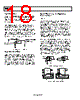
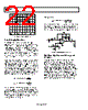
18 / 24 page  AD8067 Rev. 0 | Page 18 of 24 Input Protection Layout, Grounding, and Bypassing Considerations The inputs of the AD8067 are protected with back-to-back diodes between the input terminals as well as ESD diodes to either power supply. The result is an input stage with picoamp level input currents that can withstand 2 kV ESD events (human body model) with no degradation. LAYOUT In extremely low input bias current amplifier applications, stray leakage current paths must be kept to a minimum. Any voltage differential between the amplifier inputs and nearby traces will set up a leakage path through the PCB. Consider a 1 V signal and 100GΩ to ground present at the input of the amplifier. The resultant leakage current is 10 pA; this is ten times the input bias current of the amplifier. Poor PCB layout, contamination, and the board material can create large leakage currents. Common contaminants on boards are skin oils, moisture, solder flux, and cleaning agents. Therefore, it is imperative that the board be thoroughly cleaned and the board surface be free of contaminants to fully take advantage of the AD8067’s low input bias currents. Excessive power dissipation through the protection devices will destroy or degrade the performance of the amplifier. Differential voltages greater than 0.7 V will result in an input current of approximately (| V+ – V– | – 0.7 V)/(RI + RG)), where RI and RG are the resistors (see Figure 46). For input voltages beyond the positive supply, the input current will be about (VI – VCC – 0.7 V)/RI. For input voltages beyond the negative supply, the input current will be about (VI – VEE + 0.7 V)/RI. For any of these conditions, RI should be sized to limit the resulting input current to 50 mA or less. VI RI > (VI – VEE + 0.7V)/50mA RI > (VI – VCC – 0.7V)/50mA FOR VI BEYOND SUPPLY VOLTAGES VOUT – + RG RF RI – + AD8067 RI > ( |V+ – V– | –0.7V)/50mA FOR LARGE |V+ – V– | To significantly reduce leakage paths, a guard ring/shield around the inputs should be used. The guard ring circles the input pins and is driven to the same potential as the input signal, thereby reducing the potential difference between pins. For the guard ring to be com- pletely effective, it must be driven by a relatively low impedance source and should completely surround the input leads on all sides, above, and below, using a multilayer board (see Figure 47). The SOT-23-5 package presents a challenge in keeping the leakage paths to a minimum. The pin spacing is very tight, so extra care must be used when constructing the guard ring (see Figure 48 for recommended guard-ring construction). Figure 46. Current Limiting Resistor Capacitive Load Drive Capacitive load introduces a pole in the amplifier loop response due to the finite output impedance of the amplifier. This can cause excessive peaking and ringing in the response. The AD8067 with a gain of +10 will handle up to a 30 pF capacitive load without an excessive amount of peaking (see Figure 8). If greater capacitive load drive is required, consider inserting a small resistor in series with the load (24.9 Ω is a good value to start with). Capacitive load drive capability also increases as the gain of the amplifier increases. NON-INVERTING GUARD RING INVERTING GUARD RING Figure 47. Guard-Ring Configurations +V –IN +IN –V VOUT AD8067 NONINVERTING +V –IN +IN –V VOUT AD8067 INVERTING Figure 48. Guard-Ring Layout SOT-23-5 |
|
|
链接网址 |
| ALLDATASHEET是否为您带来帮助? [ DONATE ] |
关于 Alldatasheet | 广告服务 | 联系我们 | 隐私政策 | 数据表链接 | 链接交换 | 制造商名单 All Rights Reserved©Alldatasheet.com |
| Russian : Alldatasheetru.com | Korean : Alldatasheet.co.kr | Spanish : Alldatasheet.es | French : Alldatasheet.fr | Italian : Alldatasheetit.com Portuguese : Alldatasheetpt.com | Polish : Alldatasheet.pl | Vietnamese : Alldatasheet.vn Indian : Alldatasheet.in | Mexican : Alldatasheet.com.mx | British : Alldatasheet.co.uk | New Zealand : Alldatasheet.co.nz |
|
Family Site : ic2ic.com |
icmetro.com |
 Chinese ▼
 English
 Chinese
 German
 Japanese
 Russian
 Korean
 Spanish
 French
 Italian
 Portuguese
 Polish
 Vietnamese
 Indian
 Mexican
 British
 New Zealand