|
数据搜索系统,热门电子元器件搜索 |
|
|
数据搜索系统,热门电子元器件搜索 |
|
AD8067ART-R2 数据表(PDF) 21 Page - Analog Devices |
|
|
|||||||||||||||||||||||||||||
AD8067ART-R2 数据表(HTML) 21 Page - Analog Devices |
|
|
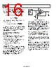
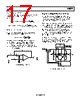
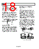
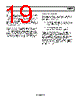
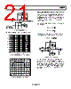
21 / 24 page  AD8067 Rev. 0 | Page 21 of 24 AD8067 0.1 µF 10 µF +5V 49.9k Ω 50 Ω 49.9k Ω 0.33pF VOUT 0.1 µF 10 µF –5V EPM 605 LL –5V 0.33pF NOTES ID @ –5V = 0.074nA CD @ –5V = 0.690pF RB @ 1550nm = –49dB Using the AD8067 at Gains of Less Than 8 A common technique used to stabilize decompensated amplifiers is to increase the noise gain, independent of the signal gain. The AD8067 can be used for signal gains of less than 8, provided that proper care is taken to ensure that the noise gain of the amplifier is set to at least the recommended minimum signal gain of 8 (See Figure 54). The signal and noise gain equations for a noninverting amplifier are shown below. 1 3 1 R R Gain Signal + = 1 3 1 R R Gain Noise + = Figure 51. Photodiode Preamplifier Test data for the preamp is shown in Figure 52 and Figure 53. The addition of resistor R2 modifies the noise gain equation, as shown below. Note the signal gain equation has not changed. FREQUENCY – MHz 100 65 70 75 80 85 90 95 60 0.01 0.1 1 10 100 2 1 3 1 R || R R Gain Noise + = AD8067 C2 0.1 µF C1 10 µF +5V R2 50 Ω C4 0.1 µF C3 10 µF –5V VOUT RL R4 51 Ω R3 600 Ω VIN 1 5 4 3 2 R1 301 Ω Figure 52. Photodiode Preamplifier Frequency Response Figure 54. Gain of Less than 2 Schematic M 50ns CH1 830mV CH1 500mV C1 RISE 31.2ns C1 FALL 31.6ns T This technique allows the designer to use the AD8067 in gain configurations of less than 8. The drawback to this type of compensation is that the input noise and offset voltages are also amplified by the value of the noise gain. In addition, the distortion performance will be degraded. To avoid excessive overshoot and ringing when driving a capacitive load, the AD8067 should be buffered by a small series resistor; in this case, a 51 Ω resistor was used. Figure 53. Photodiode Preamplifier Pulse Response |
|
|
链接网址 |
| ALLDATASHEET是否为您带来帮助? [ DONATE ] |
关于 Alldatasheet | 广告服务 | 联系我们 | 隐私政策 | 数据表链接 | 链接交换 | 制造商名单 All Rights Reserved©Alldatasheet.com |
| Russian : Alldatasheetru.com | Korean : Alldatasheet.co.kr | Spanish : Alldatasheet.es | French : Alldatasheet.fr | Italian : Alldatasheetit.com Portuguese : Alldatasheetpt.com | Polish : Alldatasheet.pl | Vietnamese : Alldatasheet.vn Indian : Alldatasheet.in | Mexican : Alldatasheet.com.mx | British : Alldatasheet.co.uk | New Zealand : Alldatasheet.co.nz |
|
Family Site : ic2ic.com |
icmetro.com |
 Chinese ▼
 English
 Chinese
 German
 Japanese
 Russian
 Korean
 Spanish
 French
 Italian
 Portuguese
 Polish
 Vietnamese
 Indian
 Mexican
 British
 New Zealand