|
数据搜索系统,热门电子元器件搜索 |
|
|
数据搜索系统,热门电子元器件搜索 |
|
ADRF6520ACPZ-R7 数据表(PDF) 8 Page - Analog Devices |
|
|
|||||||||||||||||||||||||||||
ADRF6520ACPZ-R7 数据表(HTML) 8 Page - Analog Devices |
|
|
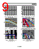
8 / 29 page  ADRF6520 Data Sheet Rev. 0 | Page 8 of 29 TYPICAL PERFORMANCE CHARACTERISTICS VPS, VPSD = 3.3 V, TA = 25°C, ZLOAD = 100 Ω, dc offset correction loop disable bit (B5) = 1 (enabled), noise spectral density (NSD) measured at fC/2 and at 500 MHz in bypass mode, unless otherwise noted. Noise figure measured with 100 Ω differential input termination. Worst case IMD3 tone is reported for all IMD3/IP3 plots. 25 20 15 10 5 0 –5 –10 0 0.25 0.50 0.75 1.00 1.25 1.50 VGN1 (V) –40°C +25°C +85°C Figure 3. Gain at 500 MHz vs. VGN1 over Temperature; Bypass Mode, VGN2 = 0 V 60 50 40 30 20 0 0.25 0.50 0.75 1.00 1.25 1.50 VGN2 (V) –40°C +25°C +85°C Figure 4. Gain at 500 MHz vs. VGN2 over Supply; Bypass Mode, VGN1 = 1.5 V 25 20 15 10 5 0 –5 –10 0 0.25 0.50 0.75 1.00 1.25 1.50 VGN1 (V) 3.3V 3.45V 3.15V Figure 5. Gain at 500 MHz vs. VGN1 over Supply; Bypass Mode, VGN2 = 0 V 3 –3 –2 –1 0 1 2 0 0.25 0.50 0.75 1.00 1.25 1.50 VGN1 (V) –40°C +25°C +85°C Figure 6. Gain Error at 500 MHz vs. VGN1 over Temperature; Bypass Mode, VGN2 = 0 V 5 –5 –4 –3 –2 –1 0 1 3 2 4 0 0.25 0.50 0.75 1.00 1.25 1.50 VGN2 (V) –40°C +25°C +85°C Figure 7. Gain Error at 500 MHz vs. VGN2 over Temperature; Bypass Mode, VGN1 = 1.5 V 60 50 40 30 20 0 0.25 0.50 0.75 1.00 1.25 1.50 VGN2 (V) 3.3V 3.45V 3.15V Figure 8. Gain at 500 MHz vs. VGN2 over Supply; Bypass Mode, VGN1 = 1.5 V |
|
|
链接网址 |
| ALLDATASHEET是否为您带来帮助? [ DONATE ] |
关于 Alldatasheet | 广告服务 | 联系我们 | 隐私政策 | 数据表链接 | 链接交换 | 制造商名单 All Rights Reserved©Alldatasheet.com |
| Russian : Alldatasheetru.com | Korean : Alldatasheet.co.kr | Spanish : Alldatasheet.es | French : Alldatasheet.fr | Italian : Alldatasheetit.com Portuguese : Alldatasheetpt.com | Polish : Alldatasheet.pl | Vietnamese : Alldatasheet.vn Indian : Alldatasheet.in | Mexican : Alldatasheet.com.mx | British : Alldatasheet.co.uk | New Zealand : Alldatasheet.co.nz |
|
Family Site : ic2ic.com |
icmetro.com |
 Chinese ▼
 English
 Chinese
 German
 Japanese
 Russian
 Korean
 Spanish
 French
 Italian
 Portuguese
 Polish
 Vietnamese
 Indian
 Mexican
 British
 New Zealand