|
数据搜索系统,热门电子元器件搜索 |
|
|
数据搜索系统,热门电子元器件搜索 |
|
ATSAM9708 数据表(PDF) 5 Page - ATMEL Corporation |
|
|
|||||||||||||||||||||||||||||
ATSAM9708 数据表(HTML) 5 Page - ATMEL Corporation |
|
|
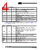
5 / 31 page  5 1772E–DRMSD–10-Apr-06 ATSAM9708 Note: 1. Memory group pins are powered by VCC2 power rail. Note: 1. X2 cannot be used to drive external circuitry. RAS 1 I/O DRAM/SDRAM row address strobe. At the end of reset RAS is tested to determine memory type configuration (pulled high to select SDRAM type). RAS should be pulled to VCC or GND through an external 10K resistor. CAS 1 I/O DRAM/SDRAM column address strobe. At the end of reset CAS is tested to determine memory type configuration (pulled high to select DRAM type). CAS should be pulled to VCC or GND through an external 10K resistor. REFRESH 1 I/O Indicates that a DRAM/SDRAM memory refresh cycle is in progress. To be used with multiple SIMM/DIMM modules to force refresh simultaneously on all modules. At the end of reset REFRESH is tested to select bootstrap state (pulled high to start built-in CPU bootstrap in case of ROMless applications). Table 3-4. Memory Group (1) (Continued) Name Pin Count Type Function Table 3-5. Miscellaneous Group Name Pin Count Type Function LFT 1 ANA PLL low pass filter. Should be connected to an external RC network. TEST 1 IN Test pin. Should be returned to GND. LDTEST 1 IN Test pin. Should be returned to GND. PDWN 1 IN Power down, active low RESET 1 IN Master reset input, active low. Schmidt trigger input. X1, X2(1) 2– Crystal connection. Crystal frequency should be fS x 256 (typ 11.2896 MHz). Crystal frequency is internally multiplied by 4 to provide the IC master clock. X1 can also be used as external clock input (3.3V input). |
|
链接网址 |
| ALLDATASHEET是否为您带来帮助? [ DONATE ] |
关于 Alldatasheet | 广告服务 | 联系我们 | 隐私政策 | 数据表链接 | 链接交换 | 制造商名单 All Rights Reserved©Alldatasheet.com |
| Russian : Alldatasheetru.com | Korean : Alldatasheet.co.kr | Spanish : Alldatasheet.es | French : Alldatasheet.fr | Italian : Alldatasheetit.com Portuguese : Alldatasheetpt.com | Polish : Alldatasheet.pl | Vietnamese : Alldatasheet.vn Indian : Alldatasheet.in | Mexican : Alldatasheet.com.mx | British : Alldatasheet.co.uk | New Zealand : Alldatasheet.co.nz |
|
Family Site : ic2ic.com |
icmetro.com |
 Chinese ▼
 English
 Chinese
 German
 Japanese
 Russian
 Korean
 Spanish
 French
 Italian
 Portuguese
 Polish
 Vietnamese
 Indian
 Mexican
 British
 New Zealand