|
数据搜索系统,热门电子元器件搜索 |
|
|
数据搜索系统,热门电子元器件搜索 |
|
NCV7728DPAR2G 数据表(PDF) 8 Page - ON Semiconductor |
|
|
|||||||||||||||||||||||||||||
NCV7728DPAR2G 数据表(HTML) 8 Page - ON Semiconductor |
|
|
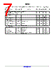
8 / 27 page  NCV7728 www.onsemi.com 8 ELECTRICAL CHARACTERISTICS (−40 °C < TJ < 150°C, 5.5 V < VSx < 40 V, 3.15 < Vcc < 5.25 V, EN= Vcc, unless otherwise specified) Characteristic Symbol Conditions Timing Chart Min Typ Max Unit DRIVER OUTPUT TIMING SPECIFICATIONS High Side Turn On Time ThsOn VSx = 13.2 V, Rload = 39 W − 7.5 13 ms High Side Turn Off Time ThsOff VSx = 13.2 V, Rload = 39 W − 3.0 6.0 ms Low Side Turn On Time TlsOn VSx = 13.2 V, Rload = 39 W − 6.5 13 ms Low Side Turn Off Time TlsOff VSx = 13.2 V, Rload = 39 W − 2.0 6.0 ms High Side Rise Time ThsTr VSx =13.2 V, Rload = 39 W − 4.0 8.0 ms High Side Fall Time ThsTf VSx = 13.2 V, Rload = 39 W − 2.0 4.0 ms Low Side Rise Time TlsTr VSx = 13.2 V, Rload = 39 W − 1.0 3.0 ms Low Side Fall Time TlsTf VSx = 13.2 V, Rload = 39 W − 1.0 3.0 ms High Side Off to Low Side On Non−Overlap Time ThsOffLsOn VSx = 13.2 V, Rload = 39 W 1.5 − − ms Low Side Off to High Side On Non−Overlap Time TlsOffHsOn VSx = 13.2 V, Rload = 39 W 1.5 − − ms SERIAL PERIPHERAL INTERFACE SCLK Frequency Fclk VCC = 5 V VCC = 3.15 V − − − − 5.0 2.0 MHz SCLK Clock Period TpClk VCC = 5 V VCC = 3.15 V 200 500 − − − − ns SCLK High Time TclkH 1 85 − − ns SCLK Low Time TclkL 2 85 − − ns SCLK Setup Time TclkSup 3 4 85 85 − − − − ns SI Setup Time TsiSup 11 50 − − ns SI Hold Time TsiH 12 50 − − ns CSB Setup Time TcsbSup 5 6 100 100 − − − − ns CSB High Time (Note 2) TcsbH 7 5.0 − − ms SO enable after CSB falling edge TenSo VCC = 5 V 8 − − 200 ns SO disable after CSB rising edge TdisSo VCC = 5 V 9 − − 200 ns SO Rise Time TsoR Cload = 40 pF Not ATE tested − − 10 25 ns SO Fall Time TsoF Cload = 40 pF Not ATE tested − − 10 25 ns SO Valid Time TsoV Cload = 40 pF SCLK ↑ to SO 50%, Not ATE tested 10 − 20 50 ns EN Low Valid Time (Note 3) TenL VCC = 5 V EN going low 50% to OUTx turing off 50% 10 − − ms EN High to SPI Valid TenHspiV − − 100 ms SRR Delay Between Two Consecutive Frame (Note 4) Tsrr 150 − − ms 2. This is the minimum time the user must wait between SPI commands. 3. This is the minimum time the user must wait before bringing EN up. 4. This is the minimum time the user must wait to send a SRR command between consecutive frames. If Tsrr time is not met the SRR request is ignored. Product parametric performance is indicated in the Electrical Characteristics for the listed test conditions, unless otherwise noted. Product performance may not be indicated by the Electrical Characteristics if operated under different conditions. |
|
|
链接网址 |
| ALLDATASHEET是否为您带来帮助? [ DONATE ] |
关于 Alldatasheet | 广告服务 | 联系我们 | 隐私政策 | 数据表链接 | 链接交换 | 制造商名单 All Rights Reserved©Alldatasheet.com |
| Russian : Alldatasheetru.com | Korean : Alldatasheet.co.kr | Spanish : Alldatasheet.es | French : Alldatasheet.fr | Italian : Alldatasheetit.com Portuguese : Alldatasheetpt.com | Polish : Alldatasheet.pl | Vietnamese : Alldatasheet.vn Indian : Alldatasheet.in | Mexican : Alldatasheet.com.mx | British : Alldatasheet.co.uk | New Zealand : Alldatasheet.co.nz |
|
Family Site : ic2ic.com |
icmetro.com |
 Chinese ▼
 English
 Chinese
 German
 Japanese
 Russian
 Korean
 Spanish
 French
 Italian
 Portuguese
 Polish
 Vietnamese
 Indian
 Mexican
 British
 New Zealand