|
数据搜索系统,热门电子元器件搜索 |
|
|
数据搜索系统,热门电子元器件搜索 |
|
NCV7728DPAR2G 数据表(PDF) 20 Page - ON Semiconductor |
|
|
|||||||||||||||||||||||||||||
NCV7728DPAR2G 数据表(HTML) 20 Page - ON Semiconductor |
|
|
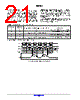
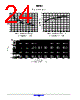
20 / 27 page  NCV7728 www.onsemi.com 20 DEVICE PROTECTION, DIAGNOSTICS AND FAULT REPORTING Power Up/Down Control Each analog power pin (VS1 or VS2) powers their respective output drivers. After a device has powered up and the output drivers are allowed to turn on, the output drivers will not turn off until the voltage on the supply pins is reduced below the initial under voltage threshold, exceeds the over voltage threshold or if shut down by either a SPI command or a fault condition. Internal power−up circuitry on the logic supply pin supports a smooth turn on transition. VCC power up resets the internal logic such that all output drivers will be off as power is applied. All the internal counters, SI and SO along with all the digital registers will be cleared on VCC POR. Exceeding the under voltage lockout threshold on VCC allows information to be input through the SPI port for turn on control. Logic information remains intact over the entire VS1 and VS2 voltage range. Under Voltage Shutdown An under voltage lockout circuit prevents the output drivers from turning on unintentionally. This control is provided by monitoring the voltages on the VS1, VS2 and VCC pins. A built−in hysteresis on the under voltage threshold is included to prevent an unknown region on the power pins; VCC, VS1 and VS2. When the VCC goes below the threshold, all outputs are turned off and the input and output registers are cleared. An under voltage condition on the VSx pins will result in shutting off all the drivers and the status bit 14 (PSF) will be set. The SPI port remains active during a VSx under−voltage if proper VCC voltage is supplied. Also all driver states will be maintained in the logic circuitry with the valid VCC voltage. Once the input voltage VSx is above the under voltage threshold level the drivers will return to programmed operation and the PSF output register bit is cleared. Under−voltage timing diagram is provided in Figure 21. Figure 21. Under−Voltage Timing Diagram OUTx LS ? OUTx LS ? X No Fault OUTx LS PSF ALL Z OUTx LS No Fault ³0x00 ALL Z VSx Vcc ? OUTx HS OUTx HS VSUV VccUV No Fault PSF No Fault 0x00 OUTx VS No Fault OUTx HS No Fault t OUTx GND OUTx GND SI Status Output State SO Z |
|
|
链接网址 |
| ALLDATASHEET是否为您带来帮助? [ DONATE ] |
关于 Alldatasheet | 广告服务 | 联系我们 | 隐私政策 | 数据表链接 | 链接交换 | 制造商名单 All Rights Reserved©Alldatasheet.com |
| Russian : Alldatasheetru.com | Korean : Alldatasheet.co.kr | Spanish : Alldatasheet.es | French : Alldatasheet.fr | Italian : Alldatasheetit.com Portuguese : Alldatasheetpt.com | Polish : Alldatasheet.pl | Vietnamese : Alldatasheet.vn Indian : Alldatasheet.in | Mexican : Alldatasheet.com.mx | British : Alldatasheet.co.uk | New Zealand : Alldatasheet.co.nz |
|
Family Site : ic2ic.com |
icmetro.com |
 Chinese ▼
 English
 Chinese
 German
 Japanese
 Russian
 Korean
 Spanish
 French
 Italian
 Portuguese
 Polish
 Vietnamese
 Indian
 Mexican
 British
 New Zealand