|
数据搜索系统,热门电子元器件搜索 |
|
|
数据搜索系统,热门电子元器件搜索 |
|
LTC4373CMS8 数据表(PDF) 9 Page - Analog Devices |
|
|
|||||||||||||||||||||||||||||
LTC4373CMS8 数据表(HTML) 9 Page - Analog Devices |
|
|
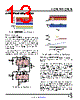
9 / 20 page  The source of the external MOSFET is connected to IN and SOURCE while its drain is connected to OUT. The LTC4372/LTC4373 control the gate of the MOSFET to regulate the voltage drop across the pass transistor to less than 30mV. In the event of a rapid drop in input voltage, such as an input short-circuit fault or negative-going voltage spike, reverse current temporarily flows through the MOSFET. This current is provided by any load capacitance and by other supplies or batteries that feed the output in diode-OR applications. The reverse current comparator quickly responds to this condition by turning the MOSFET off in 500ns. This fast turn-off prevents the reverse cur- rent from ramping up to a damaging level, thus minimiz- ing the disturbance to the output bus. IN, SOURCE and GATE are protected against reverse inputs of up to –28V. The negative comparator detects negative input potentials at SOURCE and quickly connects GATE to SOURCE, turning off the MOSFET and isolating the load from the negative input. For the LTC4372, driving SHDN high pulls the MOSFET gate down to SOURCE with a 1mA pull-down. IQ reduces to 0.5μA for a back-to-back MOSFET configuration and GATE is held low with a 3μA pull-down to GND. When SHDN goes low, the LTC4372 ramps GATE up to turn on the external MOSFET. 2UPU has a 2μA pull-up to INTVCC which can be connected to SHDN to facilitate on/off con- trol by a microcontroller’s open-drain output. The LTC4373 can monitor the input voltage via an exter- nal resistive voltage divider to UV. When UV goes below 1.191V, GATE pulls down to SOURCE with a 1mA pull- down and UVOUT pulls low. IQ reduces to 0.5μA for a back-to-back MOSFET configuration and GATE is held low with a 3μA pull down to GND. When UV recovers above VUV + VUV(HYST), the LTC4373 ramps GATE up to turn on the external MOSFET. An optional resistor can be con- nected between UV and UVOUT to configure an external hysteresis to override VUV(HYST). LTC4372/LTC4373 9 Rev. 0 For more information www.analog.com OPERATION Blocking diodes are commonly placed in series with sup- ply inputs for ORing redundant supplies and protecting against supply reversal. The LTC4372/LTC4373 replace the diodes such as in portable equipment and automo- tive applications with N-channel MOSFETs acting as ideal diodes. The forward voltage drop reduces as shown in Figure 1, a feature that is readily appreciated at low input voltages where headroom is tight. Figure 1. Forward Voltage Drop Comparison Between MOSFET and Schottky Diode VOLTAGE (V) MOSFET (BSC026N08NS5) SCHOTTKY DIODE (SBG2040CT) 0.0 0 15 10 5 20 0.3 0.4 0.5 0.1 0.2 43723 F01 As a result of this lower forward voltage drop, there is a dramatic reduction in power loss achieved in a practical application as shown in the Typical Application curve on Page 1. This represents significant savings in board area by greatly reducing heat sinking requirements of the pass device. In addition to these two desirable properties, the LTC4372/LTC4373 feature a low operating current (5µA) and shutdown current (0.5µA). This increases efficiency in applications where the ideal diode is used for intermit- tent loads or always on standby channels, making the LTC4372/LTC4373 suitable for battery powered appli- cations in the portable instrumentation, automotive and renewable energy fields. |
|
|
链接网址 |
| ALLDATASHEET是否为您带来帮助? [ DONATE ] |
关于 Alldatasheet | 广告服务 | 联系我们 | 隐私政策 | 数据表链接 | 链接交换 | 制造商名单 All Rights Reserved©Alldatasheet.com |
| Russian : Alldatasheetru.com | Korean : Alldatasheet.co.kr | Spanish : Alldatasheet.es | French : Alldatasheet.fr | Italian : Alldatasheetit.com Portuguese : Alldatasheetpt.com | Polish : Alldatasheet.pl | Vietnamese : Alldatasheet.vn Indian : Alldatasheet.in | Mexican : Alldatasheet.com.mx | British : Alldatasheet.co.uk | New Zealand : Alldatasheet.co.nz |
|
Family Site : ic2ic.com |
icmetro.com |
 Chinese ▼
 English
 Chinese
 German
 Japanese
 Russian
 Korean
 Spanish
 French
 Italian
 Portuguese
 Polish
 Vietnamese
 Indian
 Mexican
 British
 New Zealand