|
数据搜索系统,热门电子元器件搜索 |
|
|
数据搜索系统,热门电子元器件搜索 |
|
LTC4373CMS8 数据表(PDF) 16 Page - Analog Devices |
|
|
|||||||||||||||||||||||||||||
LTC4373CMS8 数据表(HTML) 16 Page - Analog Devices |
|
|
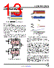
16 / 20 page  and ground to clamp IN and SOURCE when they spike neg- ative. During the input short-circuit transient, D2 diverts the reverse recovery current in the input parasitic inductances to ground while COUT does the same for the output para- sitic inductances. The 100V, FDMS86101 with RDS(ON) = 8mΩ(max) can handle both the 5A load current as well as the input short-circuit voltage transients. Figure 14 shows a high voltage application with reverse battery protection. To handle a potential worst-case situation of –48V at the input side and 48V at the out- put side, the BVDSS of the external MOSFET must be greater than 48V + 48V = 96V with allowance. Choose the 200V, IPB107N20N3G in the TO-263 package with RDS(ON) = 10.7mΩ(max). When IN is –48V and OUTPUT is 48V, D3 breaks down and clamps IN – GND at about –6V. The MOSFET is held off and isolates the load from the negative input. D1 and R7 clamps OUT – GND to about 70V. The combination of D1, D2, D3 and R7 clamps IN – OUT to about 76V. During an input short-circuit, M1 drain spikes positive and IN spikes negative. D2, D3 and D4 commutates the reverse recovery current in the input parasitic inductances while COUT does the same for the output parasitic induc- tances. D1, D2, D3, D4, R7 and R8 clamp IN, SOURCE, OUT and GND to within their Absolute Maximum Ratings. During normal ideal diode operation with GATE high, D4, C3 and C4 help to handle IQ pulsating between 300μA (charging GATE) and 3.5μA (charge pump sleep mode) while D1, D2 and D3 draw no current. LTC4372/LTC4373 16 Rev. 0 For more information www.analog.com APPLICATIONS INFORMATION Figure 13. 48V Ideal Diode without Reverse Input Protection LTC4372 OUT GATE SOURCE IN INTVCC 43723 F13 VOUT 48V 5A = 48V VIN M1 FDMS86101 COUT 10F D2 SMAJ70A 70V SHDN GND 2UPU RGND 1k C1 100nF Design Examples The following design example demonstrates the consid- erations involved in selecting components for a 12V sys- tem with 20A maximum load current (see Figure 2). First, choose the N-channel MOSFET. The 80V BSC026N08NS5 with RDS(ON) = 2.6mΩ(max) offers a good solution. The maximum voltage drop across is: ∆VSD = 20A • 2.6mΩ = 52mV The maximum power dissipation in the MOSFET is: P = 20A • 52mV = 1.04W During input short-circuit voltage transients, using the GND – GATE clamp to hold GATE should keep IN, SOURCE, GATE and OUT within their Absolute Maximum Ratings. If there is a problem with SOURCE to GND shoot through current during input short-circuits, add a RGND of 100Ω. Figure 13 shows a high voltage application. For the 48V system, using the GND – GATE clamp to hold GATE during input short-circuit voltage transients can exceed IN – OUT’s –100V absolute maximum voltage. D2 is added between IN Figure 12. Layout, MS8 and DD8 Package GND S S S G 1 2 3 4 8 7 6 5 D D D D VIN OUT VOUT MOSFET LTC4372 S S S G 1 2 3 4 8 7 6 5 D D D D VIN VOUT IN, SOURCE GATE OUT MS8 MOSFET IN, SOURCE GATE LTC4372 DD8 GND COUT CO 43723 F12 UT |
|
|
链接网址 |
| ALLDATASHEET是否为您带来帮助? [ DONATE ] |
关于 Alldatasheet | 广告服务 | 联系我们 | 隐私政策 | 数据表链接 | 链接交换 | 制造商名单 All Rights Reserved©Alldatasheet.com |
| Russian : Alldatasheetru.com | Korean : Alldatasheet.co.kr | Spanish : Alldatasheet.es | French : Alldatasheet.fr | Italian : Alldatasheetit.com Portuguese : Alldatasheetpt.com | Polish : Alldatasheet.pl | Vietnamese : Alldatasheet.vn Indian : Alldatasheet.in | Mexican : Alldatasheet.com.mx | British : Alldatasheet.co.uk | New Zealand : Alldatasheet.co.nz |
|
Family Site : ic2ic.com |
icmetro.com |
 Chinese ▼
 English
 Chinese
 German
 Japanese
 Russian
 Korean
 Spanish
 French
 Italian
 Portuguese
 Polish
 Vietnamese
 Indian
 Mexican
 British
 New Zealand