|
数据搜索系统,热门电子元器件搜索 |
|
|
数据搜索系统,热门电子元器件搜索 |
|
LTC4373CMS8 数据表(PDF) 12 Page - Analog Devices |
|
|
|||||||||||||||||||||||||||||
LTC4373CMS8 数据表(HTML) 12 Page - Analog Devices |
|
|
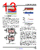
12 / 20 page  LTC4372/LTC4373 12 Rev. 0 For more information www.analog.com in LIN and LOUT is interrupted and this causes IN to spike negative and OUT to spike positive. At OUT, COUT clamps the positive going spike caused by LOUT and commutates I(LOUT) to zero. At IN, the internal GND – GATE clamp asserts and holds GATE to 32V below GND, this causes M1 to turn back on as IN/SOURCE undershoots below GATE. The current in LIN is diverted by M1 to COUT and safely commutates to zero as shown in the short-circuit transient of Figure 6b. If these transients cause too large of a ∆V at OUT, increase the capacitance of COUT or add a TVS D1. If a low source resistance power supply drives VIN, large currents can build up in LS during the short-circuit. When the short-circuit goes away, I(LS) can cause IN and SOURCE to spike positive until it is held by M1 body diode to COUT. This fast slew rate at SOURCE can cause a large shoot-through current to flow into the part from SOURCE to GND potentially causing damage. Adding an external RGND will limit this current to a safe level. For applications where IN ≤ 13.2V, a 0805 size 100Ω for RGND is sufficient. For applications where IN > 13.2V, a larger value RGND, 1k, is necessary. To keep GND from going too negative when the GND – GATE clamp turns on, a fast recovery diode like the 1N4148W is placed in parallel with the 1k RGND. For back-to-back MOSFET applications where SOURCE is not driven by VIN, RGND is not needed. RGND can also be omitted for a single MOSFET application driven by a APPLICATIONS INFORMATION power supply with a large source impedance. VIN col- lapses during the short-circuit and cannot build up cur- rent in LS. SOURCE will not see fast slew rates when the short-circuit goes away. Using the external MOSFETs to commutate the parasitic inductor currents during an input short-circuit is feasible with input voltages up to 33V. This ensures that during the transient, the IN – OUT Absolute Maximum Voltage of ±100V is not exceeded. During the short-circuit transient, the MOSFET VDS sees |VGND|+|VGATE(NEG)|+VTH(M1)+VOUT. Choose the MOSFET BVDSS accordingly. For other tech- niques to protect the LTC4372/LTC4373 during input short-circuits see the Design Examples section. Reverse Input Protection Negative voltages at IN can also occur if a battery is plugged in backwards or a negative supply is inadver- tently connected. Figure 7 shows the waveforms when the application circuit in Figure 2 is hot plugged to –24V. Due to the parasitic inductance in between input and IN/ SOURCE, the voltages at the pins can ring significantly below –24V. Similar to the input short-circuit situation, the GND – GATE clamp causes M1 to divert the current in the parasitic inductances to COUT. The GND – GATE clamp limits the maximum DC negative voltage that the Figure 2 application can handle to –28V. Figure 6. Reverse Recovery Produces Inductive Spikes at IN, SOURCE and OUT. The Polarity of Inductive Spike is Shown Across Parasitic Inductances LTC4372 OUT GATE SOURCE IN 43723 F06a VOUT VIN CLOAD M1 BSC026N08NS5 REVERSE CURRENT + – D1 SMAJ33A (OPTIONAL) LOUT OUTPUT PARASITIC INDUCTANCE COUT 10F + – LIN INPUT PARASITIC INDUCTANCE + – LS SOURCE PARASITIC INDUCTANCE INPUT SHORT D4 1N4148W (FOR VIN > 13.2V) SHDN GND RGND (a) 500ns/DIV 43723 F06b GATE, IN GND 10V/DIV I(M1) 20A/DIV 0A COUT = 10F GATE GND IN 0V (b) |
|
|
链接网址 |
| ALLDATASHEET是否为您带来帮助? [ DONATE ] |
关于 Alldatasheet | 广告服务 | 联系我们 | 隐私政策 | 数据表链接 | 链接交换 | 制造商名单 All Rights Reserved©Alldatasheet.com |
| Russian : Alldatasheetru.com | Korean : Alldatasheet.co.kr | Spanish : Alldatasheet.es | French : Alldatasheet.fr | Italian : Alldatasheetit.com Portuguese : Alldatasheetpt.com | Polish : Alldatasheet.pl | Vietnamese : Alldatasheet.vn Indian : Alldatasheet.in | Mexican : Alldatasheet.com.mx | British : Alldatasheet.co.uk | New Zealand : Alldatasheet.co.nz |
|
Family Site : ic2ic.com |
icmetro.com |
 Chinese ▼
 English
 Chinese
 German
 Japanese
 Russian
 Korean
 Spanish
 French
 Italian
 Portuguese
 Polish
 Vietnamese
 Indian
 Mexican
 British
 New Zealand