|
数据搜索系统,热门电子元器件搜索 |
|
|
数据搜索系统,热门电子元器件搜索 |
|
LTC4373CMS8 数据表(PDF) 11 Page - Analog Devices |
|
|
|||||||||||||||||||||||||||||
LTC4373CMS8 数据表(HTML) 11 Page - Analog Devices |
|
|
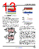
11 / 20 page  LTC4372/LTC4373 11 Rev. 0 For more information www.analog.com APPLICATIONS INFORMATION As the load current increases, GATE is driven higher and higher until a point is reached where ∆VGATE reaches the maximum overdrive that the internal charge pump is capable of (∆VGATE(H)) but ∆VSD is still above 30mV. In this situation, the internal charge pump will periodically turn on to recharge GATE as needed to keep ∆VGATE between ∆VGATE(H) and ∆VGATE(H) – 0.7V. ∆VSD is then equal to RDS(ON) • ILOAD. There is now insignificant ripple on OUT as the 0.7Vpk-pk ripple on ∆VGATE has little effect on the MOSFET RON. Achieving Low Average IQ To lower average IQ in diode control mode when GATE is high, the LTC4372/LTC4373 operate by turning on the charge pump periodically. When in charge pump sleep mode, the IQ is 3.5μA. Once the charge pump is turned on to deliver a current pulse to GATE, IQ goes up to 300μA. The average IQ will depend on how often the charge pump is turned on and this is affected by GATE leakage, GATE capacitance, OUT bypass capacitance and ILOAD. To achieve the lowest possible average IQ, mini- mize GATE leakage and ensure that GATE has a moderate capacitance (>1nF). If the CGS of the MOSFET does not already exceed this, add a 1nF capacitor between GATE and SOURCE. CLOAD may be placed nearer to the load but an OUT bypass capacitance of at least 10μF low ESR and ESL electrolytic or ceramic is required close to the drain pin of MOSFET M1 (see Figure 6a). Average IQ for Diode Control mode can be estimated by Equation 1. AVERAGEIQ = 3.5+ IGATE(LEAKAGE) IGATE(UP) • 300µA (1) The Typical Performance Characteristics section shows relationship of IQ with IGATE(LEAKAGE) and ILOAD. MOSFET Selection The LTC4372/LTC4373 drive N-channel MOSFETs to conduct the load current. The important character- istics of the MOSFET are the gate threshold voltage VGS(TH), the maximum drain-source voltage BVDSS and on-resistance RDS(ON). Gate drive is compatible with 4.5V logic-level MOSFETs over the entire operating range of 2.5V to 80V. In applica- tions with supply voltages above 5V, standard 10V thresh- old MOSFETs may be used. An internal clamp limits the gate drive to 16V maximum between GATE and SOURCE. The maximum allowable drain-source voltage, BVDSS, must be higher than the power supply voltage. If the input is grounded, the full supply voltage will appear across the MOSFET. If a reverse battery is possible and the output is held up by a charged capacitor, battery or power sup- ply, then the sum of the input and output voltages will appear across the MOSFET and BVDSS must be higher than VOUT+|VIN|. The MOSFET’s on-resistance, RDS(ON), directly affects the forward voltage drop and power dissipation during a heavy load. Desired forward voltage drop (VFWD) should be less than that of a diode for reduced power dissipa- tion; 50mV is a good starting point. Since the LTC4372/ LTC4373 drop at least 30mV across the MOSFET, a very low RDS(ON) may be wasted. Choose a MOSFET using Equation 2. RDS(ON) < VFWD ILOAD (2) The resulting power dissipation is shown in Equation 3. Pd = ILOAD2 • RDS(ON) (3) Input Short-Circuit Faults Input short-circuits that cause reverse current to flow can occur in many ways. Some examples include PCB traces getting accidentally shorted or bypass capacitors in the upstream power supply failing shorted. The LTC4372/ LTC4373 utilize the external MOSFETs to add rugged input short-circuit protection without utilizing large TVS clamps or capacitors. Figure 6a models a low impedance input short with a switch. When the short-circuit switch closes, reverse cur- rent builds up in LIN, LOUT and M1 in the direction shown. The LTC4372/LTC4373 detect the reverse current quickly and activate the internal 130mA GATE to SOURCE pull- down current to turn M1 off. The reverse current build up |
|
|
链接网址 |
| ALLDATASHEET是否为您带来帮助? [ DONATE ] |
关于 Alldatasheet | 广告服务 | 联系我们 | 隐私政策 | 数据表链接 | 链接交换 | 制造商名单 All Rights Reserved©Alldatasheet.com |
| Russian : Alldatasheetru.com | Korean : Alldatasheet.co.kr | Spanish : Alldatasheet.es | French : Alldatasheet.fr | Italian : Alldatasheetit.com Portuguese : Alldatasheetpt.com | Polish : Alldatasheet.pl | Vietnamese : Alldatasheet.vn Indian : Alldatasheet.in | Mexican : Alldatasheet.com.mx | British : Alldatasheet.co.uk | New Zealand : Alldatasheet.co.nz |
|
Family Site : ic2ic.com |
icmetro.com |
 Chinese ▼
 English
 Chinese
 German
 Japanese
 Russian
 Korean
 Spanish
 French
 Italian
 Portuguese
 Polish
 Vietnamese
 Indian
 Mexican
 British
 New Zealand