|
数据搜索系统,热门电子元器件搜索 |
|
|
数据搜索系统,热门电子元器件搜索 |
|
LTC4373CMS8 数据表(PDF) 10 Page - Analog Devices |
|
|
|||||||||||||||||||||||||||||
LTC4373CMS8 数据表(HTML) 10 Page - Analog Devices |
|
|
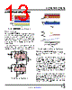
10 / 20 page  LTC4372/LTC4373 10 Rev. 0 For more information www.analog.com The LTC4372/LTC4373 operate from 2.5V to 80V and withstands an absolute maximum range of –28V to 100V without damage. In automotive applications the LTC4372/ LTC4373 can operate through load dump, cold crank and two-battery jump starts, and survive reverse battery con- nections while protecting the load. A 12V/20A ideal diode application is shown in Figure 2. The following sections cover power-on, ideal diode oper- ation, shutdown and various faults that the LTC4372/ LTC4373 detect and act upon. APPLICATIONS INFORMATION Figure 2. 12V/20A Ideal Diode with Reverse Input Protection Power-On and Ideal Diode Operation When power is applied, the initial load current flows through the body diode of the MOSFET M1. When IN exceeds the UVLO level of 2.1V and SHDN is low or UV is high, the LTC4372/LTC4373 begin operation. An internal charge pump asserts a 20µA pull-up on GATE to enhance the MOSFET. To achieve a low supply current, the LTC4372/ LTC4373 employ a pulsed control style of operation where the internal charge pump is not always on. Instead, the charge pump periodically wakes up to recharge GATE after it droops from leakage to keep ∆VSD ≤ 30mV. This pulsed control creates a voltage ripple at OUT even with a stable DC load. The amplitude of this ripple is dependent on gate leakage, GATE capacitance, the load condition and the size of the bypass capacitance at OUT. At low load or no-load condition, this ripple can increase to 30mVPK–PK. Figure 3 shows a typical OUT ripple at an ultralight ILOAD of 1µA for the circuit shown in Figure 2. With a moderate DC load, the ripple amplitude is about 10mVpk-pk. Figure 4 shows a typical OUT ripple at a mod- erate ILOAD of 2A for the circuit shown in Figure 2. Figure 3. Regulating ∆VSD at Low ILOAD = 1µA Figure 4. Regulating ∆VSD at Moderate ILOAD = 2A Figure 5. Regulating ∆VGATE at High ILOAD = 16A 50ms/DIV 43723 F03 IN, OUT 20mV/DIV IN, GATE 5V/DIV 12V 12V IGATE(LEAKAGE) = 100nA OUT GATE IN IN 5ms/DIV 43723 F04 IN, OUT 20mV/DIV IN, GATE 5V/DIV 12V 12V IGATE(LEAKAGE) = 100nA OUT GATE IN IN 10ms/DIV 43723 F05 IN, OUT 20mV/DIV IN, GATE 5V/DIV 12V 12V IGATE(LEAKAGE) = 100nA OUT GATE IN IN COUT 10F C1 100nF LTC4372 SHDN GND OUT GATE = 12V SOURCE IN 2UPU INTVCC 43723 F01 VOUT 12V 20A VIN M1 BSC026N08NS5 Figure 5 shows a typical OUT ripple at an ILOAD of 16A for the circuit shown in Figure 2. |
|
|
链接网址 |
| ALLDATASHEET是否为您带来帮助? [ DONATE ] |
关于 Alldatasheet | 广告服务 | 联系我们 | 隐私政策 | 数据表链接 | 链接交换 | 制造商名单 All Rights Reserved©Alldatasheet.com |
| Russian : Alldatasheetru.com | Korean : Alldatasheet.co.kr | Spanish : Alldatasheet.es | French : Alldatasheet.fr | Italian : Alldatasheetit.com Portuguese : Alldatasheetpt.com | Polish : Alldatasheet.pl | Vietnamese : Alldatasheet.vn Indian : Alldatasheet.in | Mexican : Alldatasheet.com.mx | British : Alldatasheet.co.uk | New Zealand : Alldatasheet.co.nz |
|
Family Site : ic2ic.com |
icmetro.com |
 Chinese ▼
 English
 Chinese
 German
 Japanese
 Russian
 Korean
 Spanish
 French
 Italian
 Portuguese
 Polish
 Vietnamese
 Indian
 Mexican
 British
 New Zealand