10 / 21 page
INGT165B / INGR165B
10/2003 - rev. 2.0
10 of 21
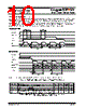
3.2.5 FLAGI / FLAGO Timing
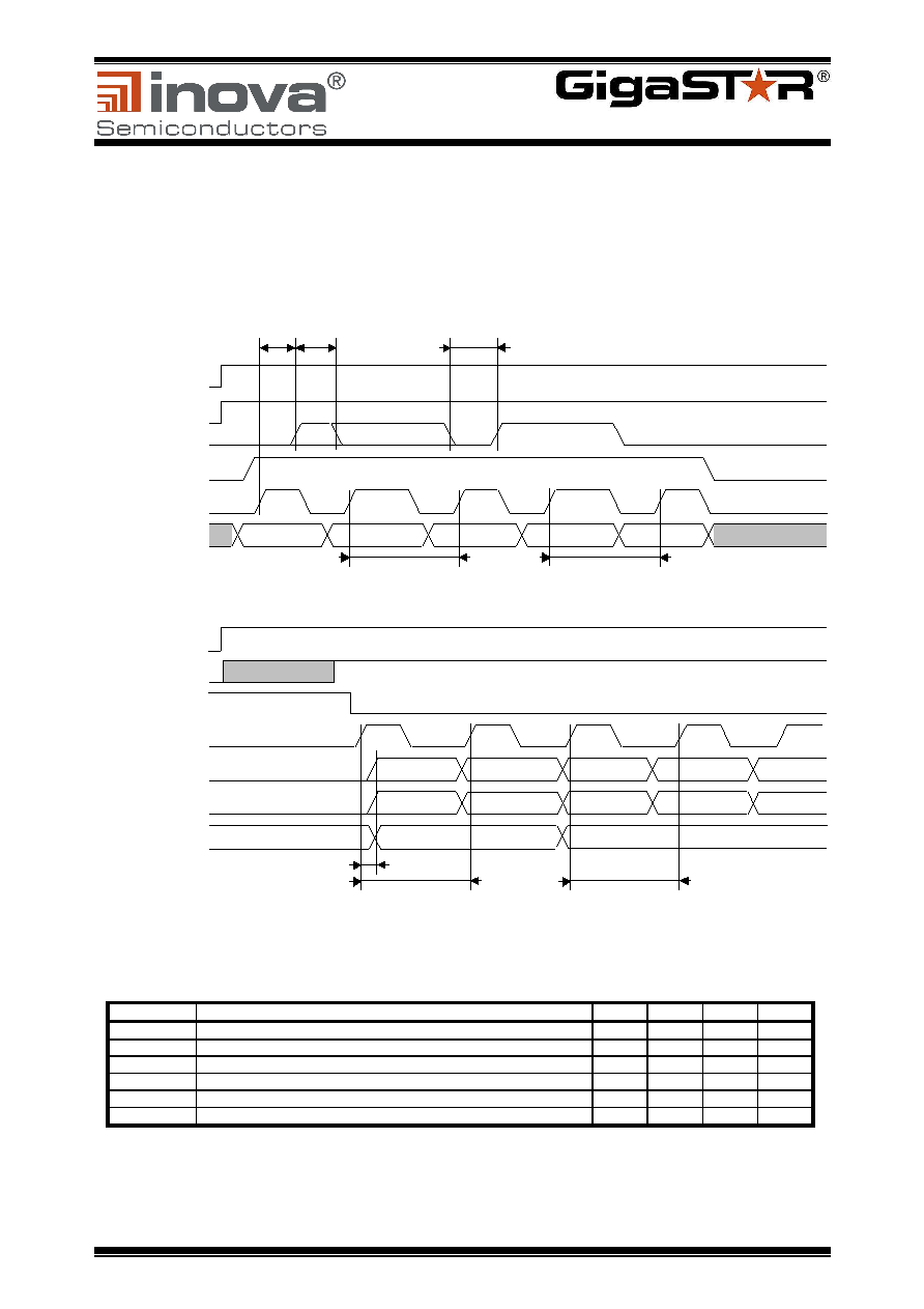
With the FLAGI / FLAGO signals a mechanism is provided to implement a sideband signalling. Each rising
edge at the Transmitter’s input FLAGI toggles the FLAGO output of the Receiver. The timing diagram for
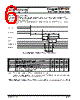
the FLAGI/FLAGO signal is shown in combination with the Transmitter signals. Note that when the FLAGI
signal is asserted, the following RDCLK high state time span is enlarged by app. 6 ns. At the Receiver, the
WRCLK low state time span is enlarged by app. 6 ns when the FLAGO output toggles. In the diagrams
below, the PARGEN is active at the Transmitter, therefore no external parity is provided.
Note : * indicates the data words [DW1, DW3] that are marked by the FLAGI signal.
Figure 10: INGT165B / INGR165B FLAGI and FLAGO Timing Diagram
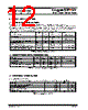
Parameter
Description
Min.
Typ.
Max.
Unit
t15
Rising edge of RDCLK to rising edge of FLAGI
0
18
ns
t16
FLAGI minimum high state
4
6
ns
t17
FLAGI minimum low state
4
6
ns
t18
RDCLK cycle time after assertion of FLAGI (one cycle only)
36
ns
t19
Rising edge of WRCLK to PDATA, PARITY and FLAGO valid
1
4
ns
t20
WRCLK cycle time for data word marked by FLAGO toggle
36
ns
Table 5: INGT165B / INGR165B FLAGI and FLAGO Timing Parameters
(under recommended operating conditions)
RECEIVER
RESET#
LOCK
LSYNC#
WRCLK
PDATA [35..0]
DW1*
DW2
DW3*
DW4
DW5...
FLAGO
PARITY
PARITY1
PARITY2
PARITY3
PARITY4
PARITY5...
RESET#
FLAGI
PARGEN
VALID
RDCLK
PDATA [35..0]
DW1*
DW2
DW3*
DW4
DW5
t15 t16
TRANSMITTER
t17
19
t
t18
t18
t20
t20

 Chinese ▼
 English
 Chinese
 German
 Japanese
 Russian
 Korean
 Spanish
 French
 Italian
 Portuguese
 Polish
 Vietnamese
 Indian
 Mexican
 British
 New Zealand