13 / 21 page
INGT165B / INGR165B
10/2003 - rev. 2.0
13 of 21
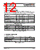
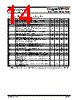
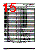
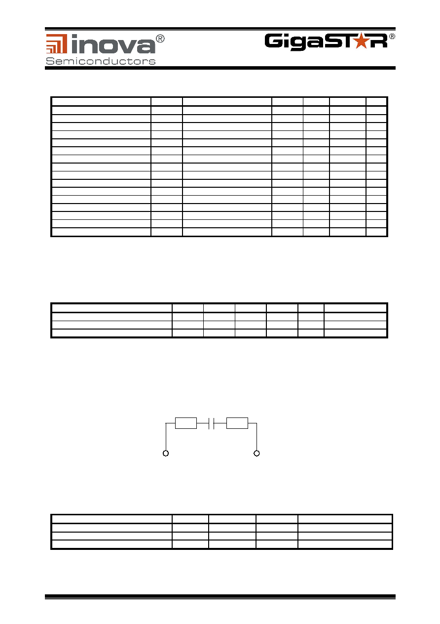
4.3.2 DC – Characteristics (under recommended operating conditions)
Parameter
Symbol
Test Condition
Min.
Typ.
Max.
Unit
CMOS Input High Voltage
VIH
2.6
V
CMOS Input Low Voltage
VIL
0.7
V
CMOS Input High Current
IIH
VIN = Vcc
-1
1
µA
CMOS Input Low Current
IIL
VIN = 0 V
-1
1
µA
EQLSEL/OSC Pin High Current IIH
VIN = Vcc
-10
40
µA
EQLSEL/OSC Pin Low Current IIL
VIN = 0 V
-10
10
µA
CMOS Output High Voltage
VOH
IOH = -0.5 mA
0,95Vcc
V
CMOS Output Low Voltage
VOL
IOL = 1.5 mA
0,05 Vcc
V
CMOS Output High Current
IOH
VOH = 0.9Vcc
-3
-5
mA
CMOS Output Low Current
IOL
VOL = 0.1Vcc
3.5
6
mA
LOCK Output High Current
ILH
VOH = 0.9Vcc
-1
-2.5
mA
LOCK Output Low Current
ILL
VOL = 0.1Vcc
1.5
3
mA
INGT165B Supply Current
ICCTX
CMOS output load = 10 pF
340
430
mA
INGR165B Supply Current
ICCRX
CMOS output load = 10 pF
300
360
mA
INGT165B Power Dissipation
PDTX
Max. data transmission rate
1.1
1.5
W
INGR165B Power Dissipation
PDRX
Max. data transmission rate
1
1.25
W
Table 11: DC – Characteristics (under recommended operating conditions)
Note : A floating CMOS input can result in heavy internal current draws. To achieve best
performance for unused inputs an external pull-up should be added.
4.3.3
Reference Clock Specification (Ta = -40 to 85° C; Vcc = 3.15 to 3.45 V)
Parameter
Symbol
Min.
Typ.
Max.
Unit
Note
Nominal Frequency
fOSC
66
MHz
Frequency Tolerance
FTOL
-100
+100
ppm
Duty Cycle
40
60
%
Table 12: Reference Clock Specification
4.3.4
External Loop Filter Specification (Ta = -40 to 85° C)
The internal PLLs of the INGT165B and the INGR165B devices require an external RC loop filter.
It is not required to use dedicated RF R- and C-components, std components will perform correctly.
Parameter
Symbol
Value Tx
Value Rx
Note
Loop Filter Capacity
CLF
1µF
1µF
Chip Capacitor (Ceramic )
Loop Filter Resistor 1
RLF1
0 Ohm
47 Ohm
Loop Filter Resistor 2
RLF2
0 Ohm
47 Ohm
Table 13: External Loop Filter Specification
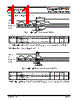
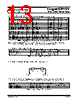
RLF1
RLF2
CLF
EXTRC1
EXTRC2

 Chinese ▼
 English
 Chinese
 German
 Japanese
 Russian
 Korean
 Spanish
 French
 Italian
 Portuguese
 Polish
 Vietnamese
 Indian
 Mexican
 British
 New Zealand