|
数据搜索系统,热门电子元器件搜索 |
|
|
数据搜索系统,热门电子元器件搜索 |
|
AD604ARSZ-R7 数据表(PDF) 14 Page - Analog Devices |
|
|
|||||||||||||||||||||||||||||
AD604ARSZ-R7 数据表(HTML) 14 Page - Analog Devices |
|
|
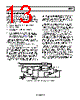
14 / 32 page  AD604 Rev. D | Page 14 of 32 PREAMPLIFIER The input capability of the following single-supply DSX (2.5 ± 2 V for a +5 V supply) limits the maximum input voltage of the preamplifier to ±400 mV for the 14 dB gain configuration or ±200 mV for the 20 dB gain configuration. The preamplifier gain can be programmed to 14 dB or 20 dB by either shorting the FBK1 node to PAO1 (14 dB) or by leaving Node FBK1 open (20 dB). These two gain settings are very accurate because they are set by the ratio of the on-chip resistors. Any intermediate gain can be achieved by connecting the appropriate resistor value between PAO1 and FBK1 according to Equation 2 and Equation 3: () 6 6 5 || 7 R R R R R V V G EXT IN OUT + + = = (2) () [] () () 6 5 6 7 7 6 5 6 R R G R R R R R G R R EXT + + × − × + − × = (3) Because the internal resistors have an absolute tolerance of ±20%, the gain can be in error by as much as 0.33 dB when REXT is 30 Ω, where it is assumed that REXT is exact. Figure 38 shows how the preamplifier is set to gains of 14 dB, 17.5 dB, and 20 dB. The gain range of a single channel of the AD604 is 0 dB to 48 dB when the preamplifier is set to 14 dB (Figure 38a), 3.5 dB to 51.5 dB for a preamp gain of 17.5 dB (Figure 38b), and 6 dB to 54 dB for the highest preamp gain of 20 dB (Figure 38c). FBK1 PAO1 COM1 PAI1 FBK1 PAO1 COM1 PAI1 FBK1 PAO1 COM1 PAI1 R6 8Ω R5 32Ω R7 40Ω a. PREAMP GAIN = 14dB b. PREAMP GAIN = 17.5dB c. PREAMP GAIN = 20dB R10 40Ω R7 40Ω R5 32Ω R6 8Ω R7 40Ω R5 32Ω R6 8Ω Figure 38. Preamplifier Gain Programmability For a preamplifier gain of 14 dB, the −3 dB small signal bandwidth of the preamplifier is 130 MHz. When the gain is at its maximum of 20 dB, the bandwidth is reduced by half to 65 MHz. Figure 39 shows the ac response for the three preamp gains shown in Figure 38. Note that the gain for an REXT of 40 Ω should be 17.5 dB, but the mismatch between the internal resistors and the external resistor causes the actual gain for this particular preamplifier to be 17.7 dB. The −3 dB small signal bandwidth of one complete channel of the AD604 (preamplifier and DSX) is 40 MHz and is independent of gain. To achieve optimum specifications, power and ground manage- ment are critical to the AD604. Large dynamic currents result because of the low resistances needed for the desired noise performance. Most of the difficulty is with the very low gain setting resistors of the preamplifier that allow for a total input referred noise, including the DSX, as low as 0.8 nV/√Hz. The consequently large dynamic currents have to be carefully handled to maintain performance even at large signal levels. 20 19 10 18 17 16 15 14 13 12 11 OPEN SHORT 50Ω 40Ω 150Ω 8Ω 32Ω IN 40Ω 100M 10M 1M 100k FREQUENCY (Hz) REXT VIN Figure 39. AC Response for Preamplifier Gains of 14 dB, 17.5 dB, and 20 dB The preamplifier uses a dual ±5 V supply to accommodate large dynamic currents and a ground referenced input. The preamplifier output is also ground referenced and requires a common-mode level shift into the single-supply DSX. The two external coupling capacitors (C1 and C2 in Figure 37) connected to the PAO1 and +DSX, and −DSX nodes and ground, respectively, perform this function (see the AC Coupling section). In addition, they eliminate any offset that would otherwise be introduced by the preamplifier. It should be noted that an offset of 1 mV at the input of the DSX is amplified by 34.4 dB (× 52.5) when the gain control voltage is at its maximum; this equates to 52.5 mV at the output. AC coupling is consequently required to keep the offset from degrading the output signal range. The gain-setting preamplifier feedback resistors are small enough (8 Ω and 32 Ω) that even an additional 1 Ω in the ground connection at Pin COM1 (the input common-mode reference) seriously degrades gain accuracy and noise performance. This node is sensitive and careful attention is necessary to minimize the ground impedance. All connections to the COM1 node should be as short as possible. The preamplifier, including the gain setting resistors, has a noise performance of 0.71 nV/√Hz and 3 pA/√Hz. Note that a significant portion of the total input referred voltage noise is due to the feedback resistors. The equivalent noise resistance presented by R5 and R6 in parallel is nominally 6.4 Ω, which contributes 0.33 nV/√Hz to the total input referred voltage noise. |
|
链接网址 |
| ALLDATASHEET是否为您带来帮助? [ DONATE ] |
关于 Alldatasheet | 广告服务 | 联系我们 | 隐私政策 | 数据表链接 | 链接交换 | 制造商名单 All Rights Reserved©Alldatasheet.com |
| Russian : Alldatasheetru.com | Korean : Alldatasheet.co.kr | Spanish : Alldatasheet.es | French : Alldatasheet.fr | Italian : Alldatasheetit.com Portuguese : Alldatasheetpt.com | Polish : Alldatasheet.pl | Vietnamese : Alldatasheet.vn Indian : Alldatasheet.in | Mexican : Alldatasheet.com.mx | British : Alldatasheet.co.uk | New Zealand : Alldatasheet.co.nz |
|
Family Site : ic2ic.com |
icmetro.com |
 Chinese ▼
 English
 Chinese
 German
 Japanese
 Russian
 Korean
 Spanish
 French
 Italian
 Portuguese
 Polish
 Vietnamese
 Indian
 Mexican
 British
 New Zealand