|
数据搜索系统,热门电子元器件搜索 |
|
|
数据搜索系统,热门电子元器件搜索 |
|
AD604ARSZ-R7 数据表(PDF) 20 Page - Analog Devices |
|
|
|||||||||||||||||||||||||||||
AD604ARSZ-R7 数据表(HTML) 20 Page - Analog Devices |
|
|
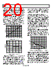
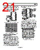
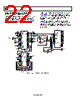
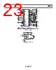
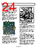
20 / 32 page  AD604 Rev. D | Page 20 of 32 The 50 Ω termination resistor, together with the 50 Ω source resistance of the signal generator, combine to an effective resistance as seen by the input of the preamplifier of 25 Ω, which makes 4.07 μV of rms noise in 40 MHz. The noise floor of this channel is consequently the rms sum of these two main noise sources, 6.5 μV rms. The minimum detectable signal (MDS) for this circuit is +6.5 μV rms (−90.7 dBm). Generally, the measured signal should be about a factor of three larger than the noise floor, in this case 19.5 μV rms. Note that the 25 μV rms signal that this AGC circuit can correct for is just slightly above the MDS. Of course, the sensitivity of the input can be improved by bandlimiting the signal; if the noise bandwidth is reduced by a factor of four to 10 MHz, the noise floor of the AGC circuit with a 50 Ω termination resistor drops to +3.25 μV rms (−96.7 dBm). Further noise improvement can be achieved by an input matching network or by transformer coupling of the input signal. VGN (V) 90 80 –30 70 60 20 50 40 30 –20 –10 0 10 f =1MHz 0.1 0.5 0.9 1.3 1.7 2.1 2.5 2.9 Figure 45. Cascaded Gain vs. VGN VGN (V) 4 3 –4 2 1 –3 0 –1 –2 f =1MHz 0.2 0.7 1.2 1.7 2.2 2.7 Figure 46. Cascaded Gain Error vs. VGN The descriptions of the detector circuitry functions, comprising a squarer, a low-pass filter, and an integrator, follow. At this point, it is necessary to make some assumptions about the input signal. The following explanation of the detector circuitry presumes an amplitude modulated RF carrier where the modulating signal is at a much lower frequency than the RF signal. The AD835 multiplier functions as the detector by squaring the output signal presented to it by the AD604. A low-pass filter following the squaring operation removes the RF signal component at twice the incoming signal frequency, while passing the low frequency AM information. The following integrator with a time constant of 2 ms set by R8 and C11 integrates the error signal presented by the low-pass filter and changes VG until the error signal is equal to VSET. For example, if the signal presented to the detector is V1 = A × cos(ωt) as indicated in Figure 44, the output of the squarer is −(V1)2/1 V. The reason for all the minus signs in the detection circuitry comes from the necessity of providing negative feedback in the control loop; actually, if VSET becomes greater than 0 V, the control loop provides positive feedback. Squaring A × cos(ωt) results in two terms, one at dc and one at 2ω; the following low-pass filter passes only the −(A)2/2 dc term. This dc voltage is now forced equal to the voltage, VSET, by the control loop. The squarer, together with the low-pass filter, functions as a mean-square detector. As should be evident by controlling the value of VSET, the amplitude of the voltage V1 can be set at the input of the AD835; if VSET equals −80 mV, the AGC output signal amplitude is ±400 mV. Figure 47 shows the control voltage, VGN, vs. the input power at frequencies of 1 MHz (solid line) and 10 MHz (dashed line) at an output regulated level of 2 dBm (800 mV p-p). The AGC threshold is evident at a PIN of about −79 dBm; the highest input power that can still be accommodated is about +3 dBm. At this level, the output starts being distorted because of clipping in the preamplifier. 4.5 4.0 0.5 3.5 3.0 1.0 2.5 2.0 1.5 1MHz 10MHz PIN (dBm) –80 –70 –60 –50 –40 –30 –20 –10 0 10 Figure 47. Control Voltage vs. Input Power of Circuit in Figure 44 As previously mentioned, the second preamplifier can be used to extend the range of the AGC circuit in Figure 44. Figure 48 shows the modifications that must be made to Figure 46 to achieve 96 dB of gain and dynamic range. Because of the extremely high gain, the bandwidth must be limited to reject some of the noise. Furthermore, limiting the bandwidth helps suppress high frequency oscillations. The added components act as a low-pass filter and dc block (C5 decouples the 2.5 V common-mode output of the first DSX). The ferrite bead has an impedance of about 5 Ω at 1 MHz, 30 Ω at 10 MHz, and 70 Ω at 100 MHz. The bead, combined with R2 and C6, forms a 1 MHz low-pass filter. |
|
链接网址 |
| ALLDATASHEET是否为您带来帮助? [ DONATE ] |
关于 Alldatasheet | 广告服务 | 联系我们 | 隐私政策 | 数据表链接 | 链接交换 | 制造商名单 All Rights Reserved©Alldatasheet.com |
| Russian : Alldatasheetru.com | Korean : Alldatasheet.co.kr | Spanish : Alldatasheet.es | French : Alldatasheet.fr | Italian : Alldatasheetit.com Portuguese : Alldatasheetpt.com | Polish : Alldatasheet.pl | Vietnamese : Alldatasheet.vn Indian : Alldatasheet.in | Mexican : Alldatasheet.com.mx | British : Alldatasheet.co.uk | New Zealand : Alldatasheet.co.nz |
|
Family Site : ic2ic.com |
icmetro.com |
 Chinese ▼
 English
 Chinese
 German
 Japanese
 Russian
 Korean
 Spanish
 French
 Italian
 Portuguese
 Polish
 Vietnamese
 Indian
 Mexican
 British
 New Zealand