|
数据搜索系统,热门电子元器件搜索 |
|
|
数据搜索系统,热门电子元器件搜索 |
|
AD604ARSZ-R7 数据表(PDF) 18 Page - Analog Devices |
|
|
|||||||||||||||||||||||||||||
AD604ARSZ-R7 数据表(HTML) 18 Page - Analog Devices |
|
|
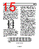
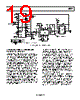
18 / 32 page  AD604 Rev. D | Page 18 of 32 APPLICATIONS INFORMATION The basic circuit in Figure 43 shows the connections for one channel of the AD604. The signal is applied at Pin 5. RGN is normally 0, in which case the preamplifier is set to a gain of 5 (14 dB). When FBK1 is left open, the preamplifier is set to a gain of 10 (20 dB) and the gain range shifts up by 6 dB. The ac coupling capacitors before −DSX1 and +DSX1 should be selected according to the required lower cutoff frequency. In this example, the 0.1 μF capacitors, together with the 175 Ω seen looking into each of the DSX input pins, provide a −3 dB high-pass corner of about 9.1 kHz. The upper cutoff frequency is determined by the bandwidth of the channel, which is 40 MHz. Note that the signal can be simply inverted by connecting the output of the preamplifier to −DSX1 instead of +DSX1; this is due to the fully differential input of the DSX. 12 11 10 9 8 1 2 3 4 7 6 5 13 16 15 14 24 23 22 21 20 19 18 17 AD604 VGN RGN +2.5V +5V –5V OUT –DSX1 +DSX1 PAI1 FBK1 PAO1 COM1 COM2 PAI2 FBK2 PAO2 +DSX2 –DSX2 VGN1 VREF VPOS GND1 OUT1 VNEG VNEG VPOS GND2 OUT2 VOCM VGN2 0.1µF 0.1µF 0.1µF VIN 0.1µF RL 500Ω Figure 43. Basic Connections for a Single Channel In Figure 43, the output is ac-coupled for optimum performance. For dc coupling, as shown in Figure 52, the capacitor can be eliminated if VOCM is biased at the same 3.3 V common- mode voltage as the analog-to-digital converter, AD9050. VREF requires a voltage of 1.25 V to 2.5 V, with between 40 dB/V and 20 dB/V gain scaling, respectively. Voltage VGN controls the gain; its nominal operating range is from 0.25 V to 2.65 V for 20 dB/V gain scaling and 0.125 V to 1.325 V for 40 dB/V scaling. When VGNx is grounded, the channel powers down and disables its output. COM1 is the main signal ground for the preamplifier and needs to be connected with as short a connection as possible to the input ground. Because the internal feedback resistors of the preamplifier are very small for noise reasons (8 Ω and 32 Ω nominally), it is of utmost importance to keep the resistance in this connection to a minimum. Furthermore, excessive inductance in this connection can lead to oscillations. Because of the ultralow noise and wide bandwidth of the AD604, large dynamic currents flow to and from the power supply. To ensure the stability of the part, extreme attention to supply decoupling is required. A large storage capacitor in parallel with a smaller high frequency capacitor connected at the supply pins, together with a ferrite bead coming from the supply, should be used to ensure high frequency stability. To provide for additional flexibility, COM1 can be used to disable the preamplifier. When COM1 is connected to VP, the preamplifier is off, yet the DSX portion can be used independently. This may be of value when cascading the two DSX stages in the AD604. In this case, the first DSX output signal with respect to noise is large and using the second preamplifier at this point would waste power (see Figure 44). |
|
链接网址 |
| ALLDATASHEET是否为您带来帮助? [ DONATE ] |
关于 Alldatasheet | 广告服务 | 联系我们 | 隐私政策 | 数据表链接 | 链接交换 | 制造商名单 All Rights Reserved©Alldatasheet.com |
| Russian : Alldatasheetru.com | Korean : Alldatasheet.co.kr | Spanish : Alldatasheet.es | French : Alldatasheet.fr | Italian : Alldatasheetit.com Portuguese : Alldatasheetpt.com | Polish : Alldatasheet.pl | Vietnamese : Alldatasheet.vn Indian : Alldatasheet.in | Mexican : Alldatasheet.com.mx | British : Alldatasheet.co.uk | New Zealand : Alldatasheet.co.nz |
|
Family Site : ic2ic.com |
icmetro.com |
 Chinese ▼
 English
 Chinese
 German
 Japanese
 Russian
 Korean
 Spanish
 French
 Italian
 Portuguese
 Polish
 Vietnamese
 Indian
 Mexican
 British
 New Zealand